Dynamic mask projection stereo micro lithography

a stereo micro lithography and dynamic mask technology, applied in the field of 3d structure microfabrication, can solve the problems of not being able to achieve the above goals, not being able to fabricate complex 3d micro parts with high aspect ratio, and most of the ic-based micromachining process cannot be used to fabricate complex 3d micro parts

Inactive Publication Date: 2006-08-08
RGT UNIV OF CALIFORNIA
View PDF10 Cites 71 Cited by
  • Summary
  • Abstract
  • Description
  • Claims
  • Application Information

AI Technical Summary

Problems solved by technology

Current IC-based micromachining processes, used to fabricate MEMS devices, have certain limitations in achieving the above goals.
First, most of the IC-based micromachining processes cannot be used to fabricate complex 3D micro parts with high aspect ratios.
Second, only a few semiconductors and other materials can be processed by the current IC-based micromachining for MEMS.
However, the x-ray LIGA process has not found a large number of industrial applications due to its poor industrial accessibility and operational cost.
In addition, complex 3D structures can not be achieved by an LIGA process.
However, due to the large pixel size and very low transmission in UV, the device's resolution is limited and contrast is poor.

Method used


Image

  • Dynamic mask projection stereo micro lithography
  • Dynamic mask projection stereo micro lithography

Examples


Embodiment Construction

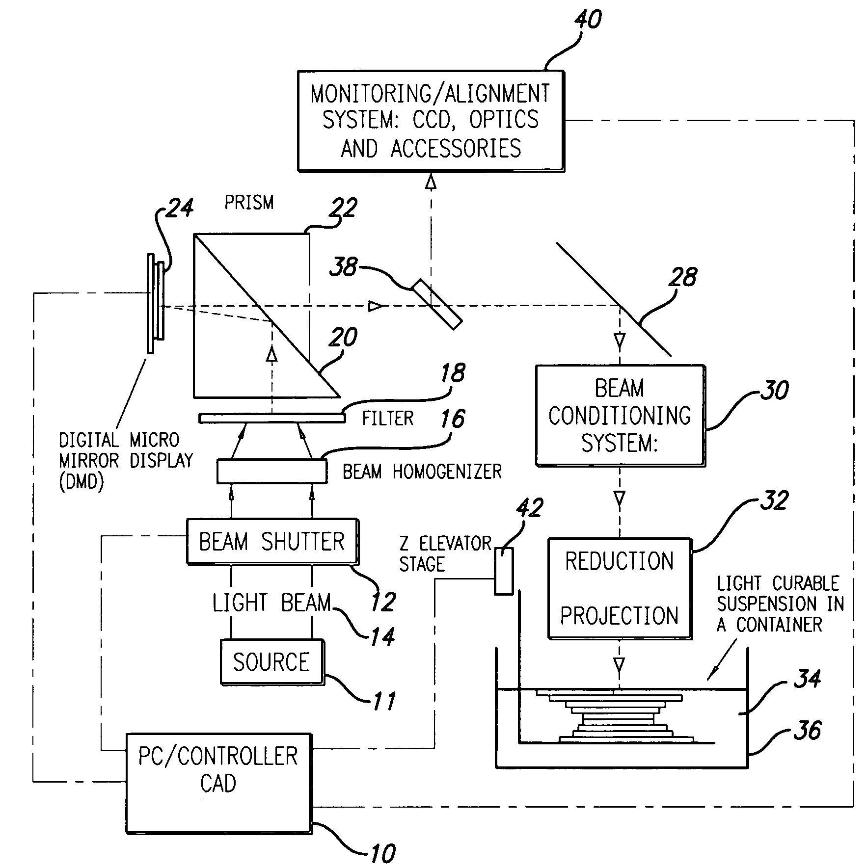
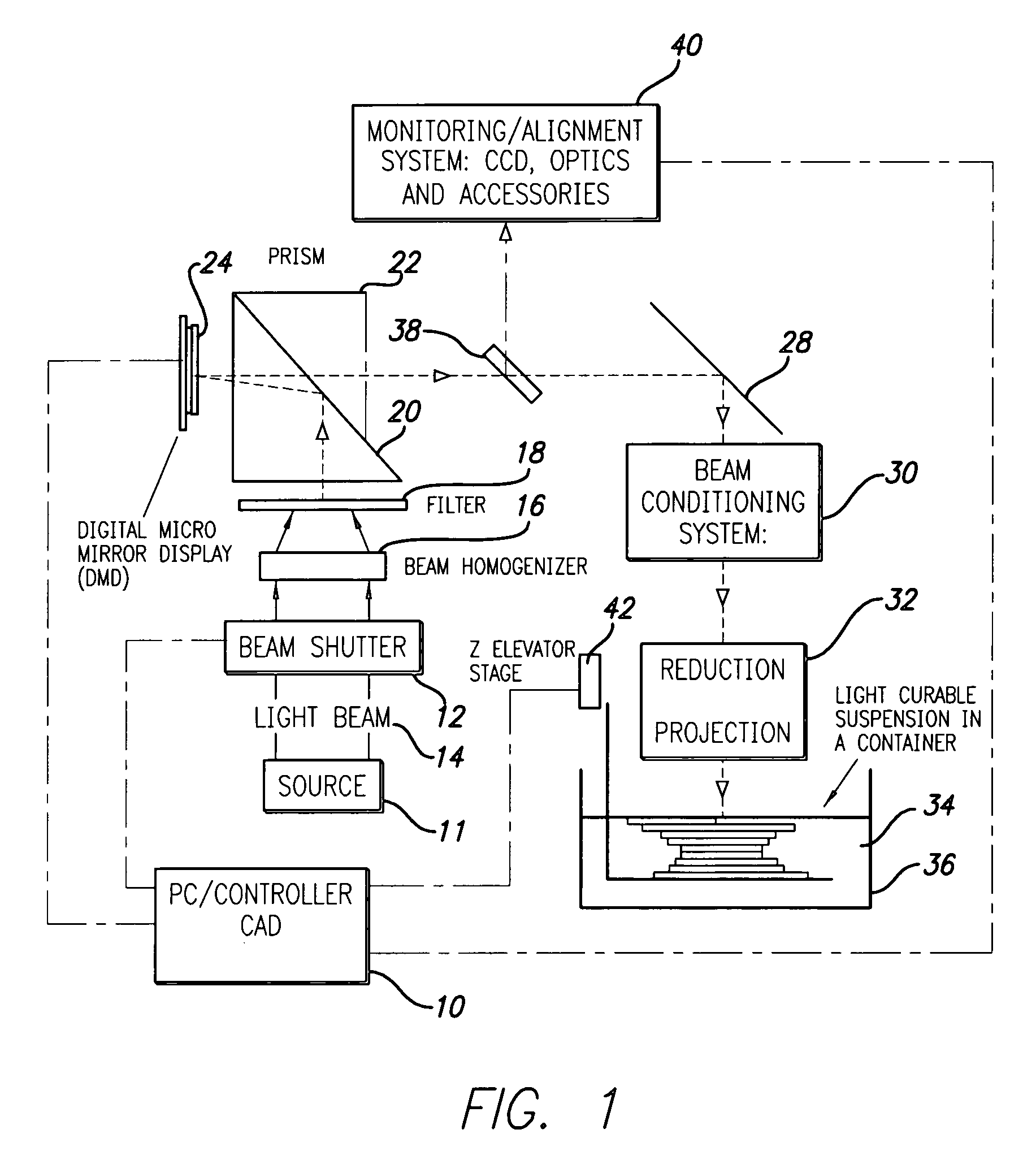
[0012]The present invention is used to fabricate 3D complex micro / nano structures by digital light processing using a dynamic mask. Digital light processing technology is a high brightness and contrast, high resolution technique composed of a micro-electro-mechanical semiconductor based array of small, fast independently hinged reflective surfaces (or mirrors) the combination of which is known as a digital micro-mirror device or display (DMD). The reflective surfaces, each of which represents a single pixel, can be of very small size, in the micrometer range, or even smaller. In a non-limiting embodiment, reflective surfaces are in the range of 0.1–17 μm. They are square mirrors that can reflect light in two directions, namely “on” and “off.” In the on position, the mirrors reflect light through the optics onto or into the object being exposed and the mirrors appear bright. Conversely, when the mirrors are in the off position, the light is reflected out of the optical field and the ...


PUM

PropertyMeasurementUnit
three-dimensional structureaaaaaaaaaa
relative vertical movementaaaaaaaaaa
vertical movementaaaaaaaaaa

Abstract

Three-dimensional structures are fabricated by a process in which a 3D solid model is designed by software at a PC and sliced into a series of 2D layers. Each 2D layer is displayed at a dynamic mask via micro-mirror deflections projected onto a photoresist to form a layer, which is lowered and the process is repeated to build the object layer by layer.

Description

CROSS REFERENCE TO RELATED APPLICATIONS[0001]This application is based on U.S. Application Ser. No. 60 / 235,799, filed Sep. 27,2000.FIELD OF THE INVENTION[0002]The field of the invention is microfabrication of 3D structuresBACKGROUND OF THE INVENTION[0003]Micro-electro-mechanical systems (MEMS) devices have been found in many sensing applications such as airbag sensors, as well as chemical and biological sensors. The use of micro actuators is the key to making MEMS fully active, intelligent “micro-system” devices, capable of both sensing and actuating. Current IC-based micromachining processes, used to fabricate MEMS devices, have certain limitations in achieving the above goals. First, most of the IC-based micromachining processes cannot be used to fabricate complex 3D micro parts with high aspect ratios. Second, only a few semiconductors and other materials can be processed by the current IC-based micromachining for MEMS. Many other important engineering materials, such as smart ce...

Claims


Application Information

Patent Timeline
Patent Type & Authority Patents(United States)
IPC IPC(8): G03B27/32B29C35/04C08J7/04G03B27/52B29C67/00G03F7/00G03F7/20G21K5/00
CPCG03F7/2057G03F7/0037B29C67/007B29C67/0062G03F7/70291G03F7/70416B29C64/124B29C64/129B33Y30/00B33Y10/00B33Y80/00
Inventor ZHANG, XIANG
Owner RGT UNIV OF CALIFORNIA
Why Eureka
Try Eureka