Ultraviolet irradiating method and an apparatus using the same

Inactive Publication Date: 2006-08-15
NITTO DENKO CORP
View PDF10 Cites 6 Cited by
  • Summary
  • Abstract
  • Description
  • Claims
  • Application Information

AI Technical Summary

Benefits of technology

[0014]According to this invention, ultraviolet light is emitted toward a work piece held by a frame through an ultraviolet sensitive adhesive tape, while the undersurface of the work piece is supported. This limits a downward displacement of the work piece due to softening of the adhesive tape under the influence of heat in time of ultraviolet irradiation and slackening under the weight of the work piece. As a result, it is possible to reduce stress imposed on the work piece by slackening of the adhesive tape, and avoid damage to the work piece held.
[0028]Further, the work piece, preferably, is a semiconductor wafer, glass component or semiconductor package substrate. That is, where a high processing accuracy is needed such as in processing precision components, an excessive stress may be prevented from occurring with each work piece in time of handling, e.g. transporting, the work piece by precluding deformation of the ultraviolet sensitive type adhesive tape.

Problems solved by technology

However, the apparatus using the conventional ultraviolet irradiating method has the following drawbacks.
Furthermore, due to the heat generated in time of ultraviolet irradiation, the adhesive tape tends to soften and become slack under the weight of such a large wafer.
Consequently, there has arisen a problem of corners of adjoining diced chips rubbing against one another to be damaged.
When intervals between the chips or packages are reduced by slackening of the adhesive tape, an operating inconvenience will occur where, for example, individual chips cannot be recognized accurately in picking up the chips with a suction collet.
Moreover, the adhesive tape which has once slackened by heat cannot be restored.
While a wafer with the adhesive tape in the slack state is transported to the bonding step, the chips could contact each other to be damaged.
When sucking chips from a wafer joined with a ring-shaped frame with a suction collet for transport, the collet may fail to suck the chips accurately, thereby damaging the chips.

Method used


Image

  • Ultraviolet irradiating method and an apparatus using the same
  • Ultraviolet irradiating method and an apparatus using the same
  • Ultraviolet irradiating method and an apparatus using the same

Examples


Embodiment Construction

[0037]A preferred embodiment of this invention will be described hereinafter with reference to the drawings.

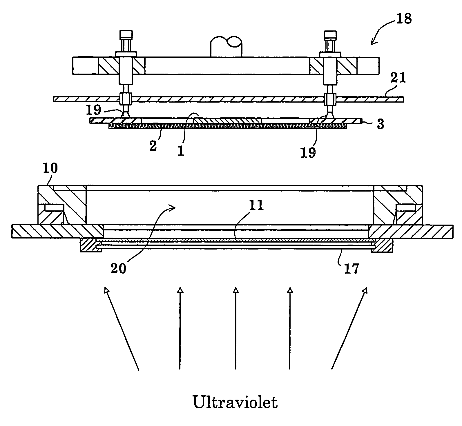
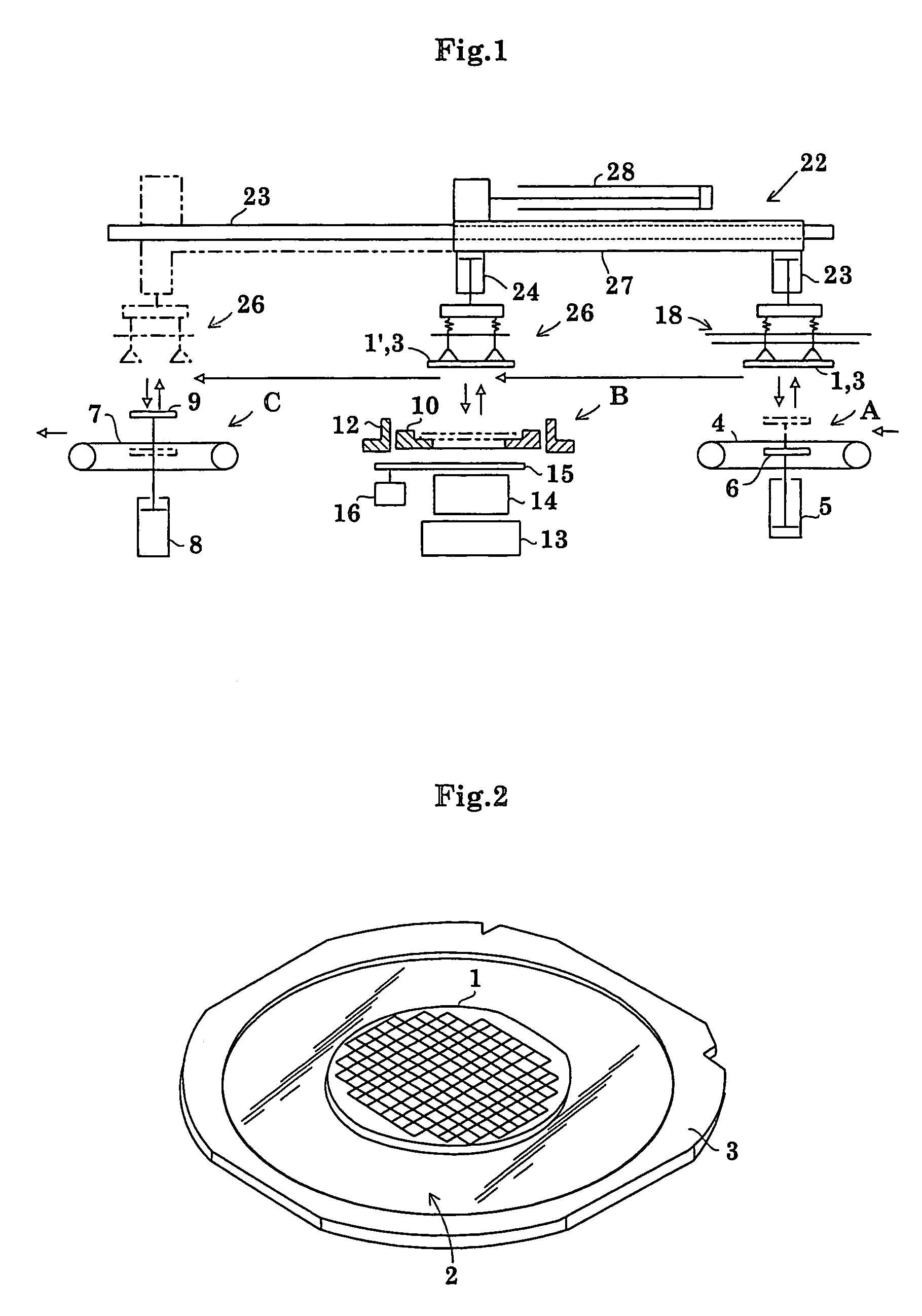
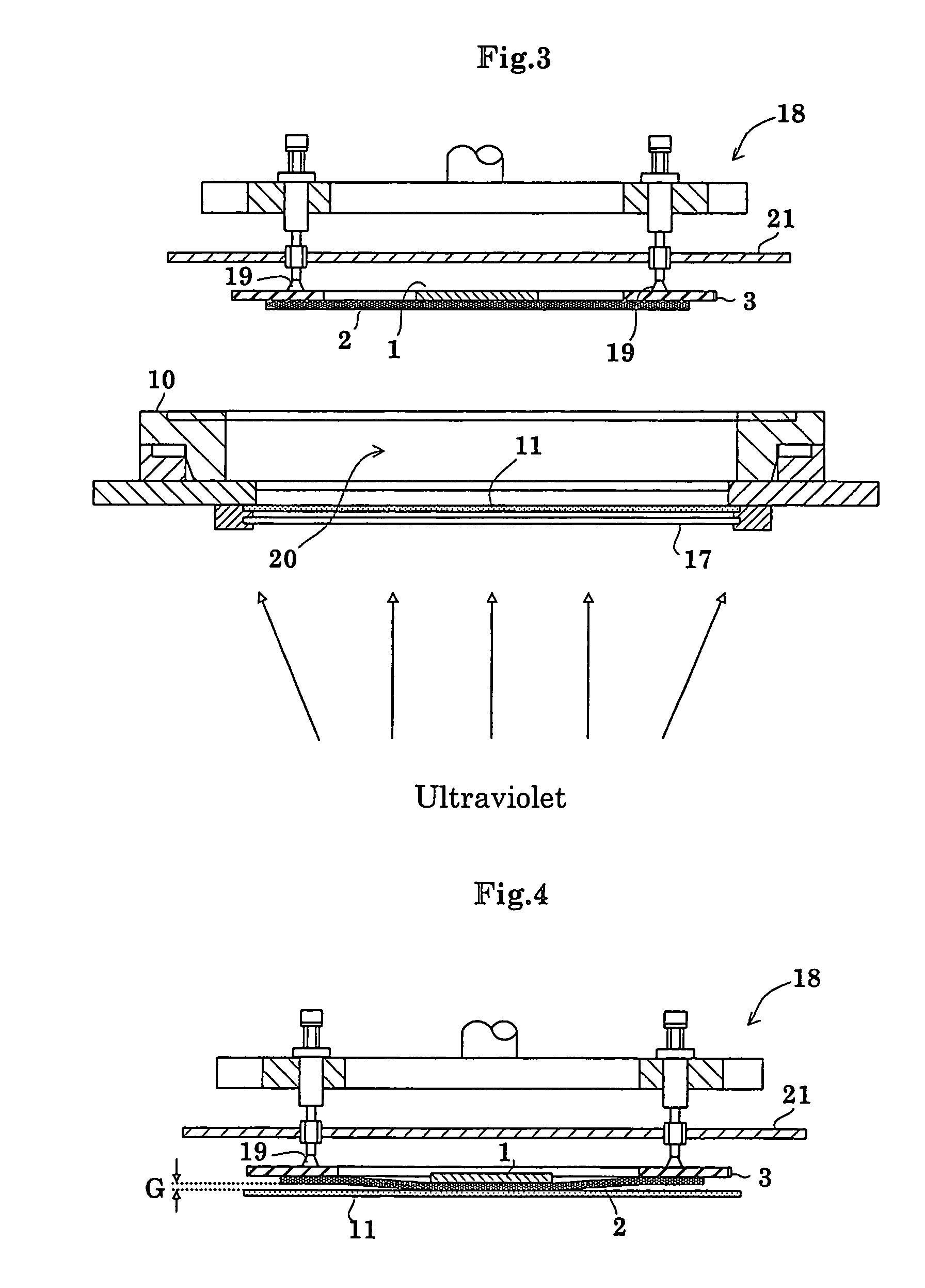
[0038]FIG. 1 is a front view showing an outline of a mechanical portion of an ultraviolet irradiating apparatus according to this invention. FIG. 2 is a perspective view of a work piece held by a frame to be processed. A semiconductor wafer (hereinafter simply called “wafer”) has an ultraviolet sensitive adhesive tape larger than the wafer applied to the back surface thereof. The adhesive tape is applied at peripheries thereof also to a ring-shaped frame. In this embodiment, the wafer is transported as integrated with the ring-shaped frame.

[0039]The ultraviolet irradiating apparatus in this embodiment includes a work piece loading section A for receiving a ring-shaped frame 3 integrated with a wafer 1 from a dicing apparatus, not shown, disposed in an upstream location, an ultraviolet irradiating section B, and a work piece unloading section C for delivering the wafer 1 after ...


PUM


Abstract

An ultraviolet irradiating apparatus for emitting ultraviolet light toward a work piece. The work piece, e.g. a semiconductor wafer, is held by a ring-shaped frame through an ultraviolet sensitive adhesive tape applied to the back surface of the wafer. The apparatus includes an ultraviolet irradiating section having a regulating member disposed in a lower position of a support base. The regulating member is provided to limit a downward displacement of the wafer.

Description

BACKGROUND OF THE INVENTION[0001](1) Field of the Invention[0002]This invention relates to an ultraviolet irradiating apparatus for emitting ultraviolet light toward a work piece such as a semiconductor wafer or electronic part and a frame holding the work piece through an ultraviolet sensitive adhesive tape applied to the back surface of the work piece.[0003](2) Description of the Related Art[0004]In a conventional process of manufacturing semiconductor wafers (hereinafter simply called “wafers”) or electronic parts, work pieces are processed as held with an ultraviolet sensitive adhesive tape applied thereto.[0005]The semiconductor manufacturing process includes a dicing step for cutting a wafer into chips, for example. In this dicing step, the wafer is mounted centrally of a ring-shaped frame, and held (supported) with an ultraviolet sensitive adhesive tape applied to the back surface of the wafer in a way to cover the ring-shaped frame as well.[0006]That is, a semiconductor wafe...

Claims


Application Information

Patent Timeline
IPC IPC(8): G01N23/00G01J1/42G01N21/64G01T1/20H01J37/20H01L21/00H01L21/301
CPCH01L21/67132H01L21/67115A47G19/186A47G2400/02
Inventor OKAWA, YUJI
Owner NITTO DENKO CORP
Why Eureka
Try Eureka