Method for manufacturing photomask and method for manufacturing semiconductor device using photomask

Inactive Publication Date: 2006-10-05
FUJITSU SEMICON LTD
View PDF8 Cites 6 Cited by
  • Summary
  • Abstract
  • Description
  • Claims
  • Application Information

AI Technical Summary

Benefits of technology

[0011] It is an object of the present invention to provide a method for manufacturing a photomask in which the time for creating data for forming a pattern on the photomask is reduced to thereby reduce the production time of the photomask, and a method for manufacturing a semiconductor device using the photomask.

Problems solved by technology

Therefore, a problem occurs in that the time for creating data for a layout pattern on the photomask becomes long and the time for manufacturing the photomask also increases.

Method used


Image

  • Method for manufacturing photomask and method for manufacturing semiconductor device using photomask
  • Method for manufacturing photomask and method for manufacturing semiconductor device using photomask
  • Method for manufacturing photomask and method for manufacturing semiconductor device using photomask

Examples


first embodiment

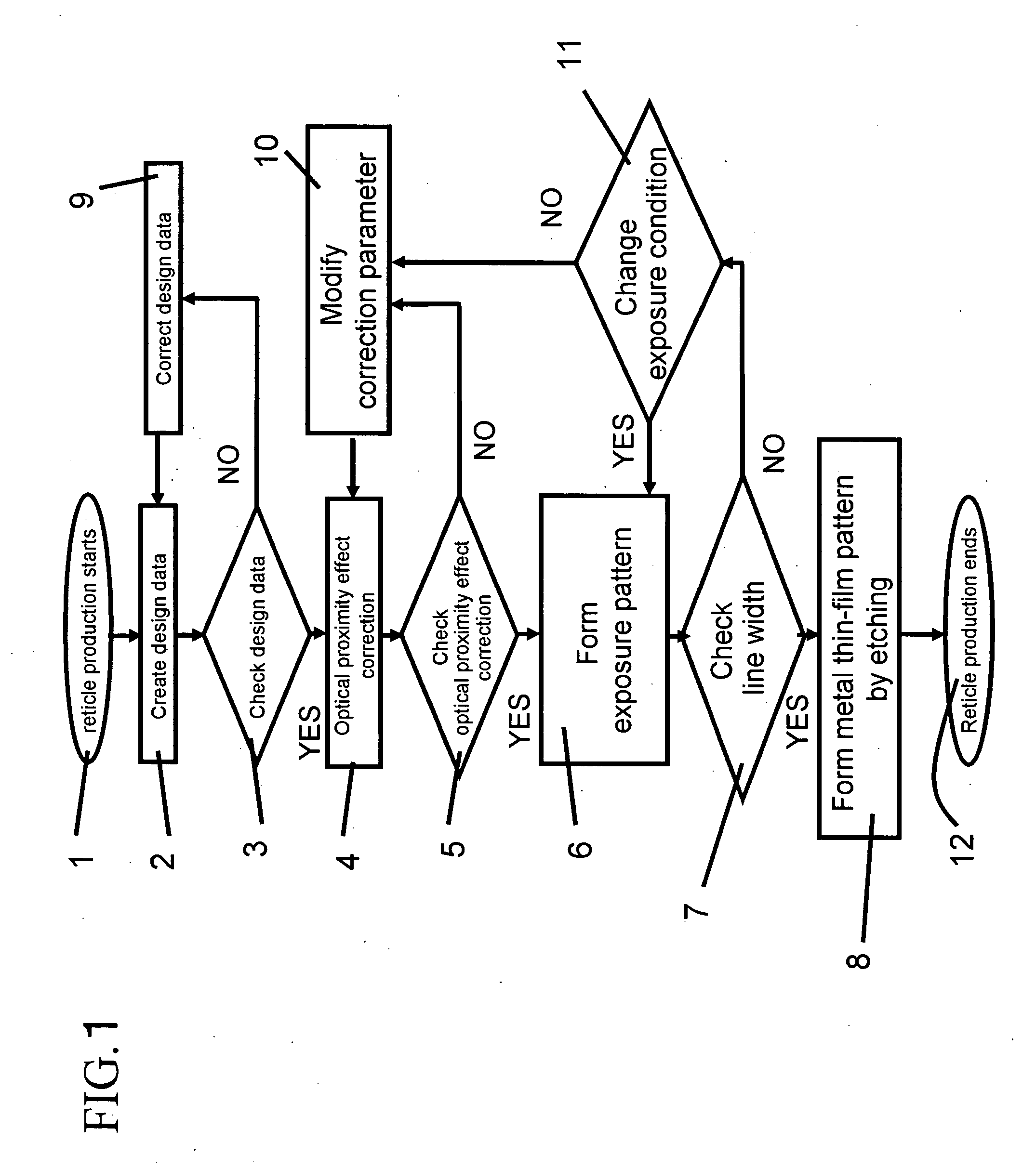
[0041] A method for manufacturing a photomask according to a first embodiment of the present invention will be described with reference to FIGS. 1 to 11. The term photomask means a sheet, typically, a quartz glass plate, having a metal thin-film pattern formed thereon. Light is applied to the photomask to transfer the metal thin-film pattern on the photomask to a photosensitive film, or a resist, applied to a semiconductor substrate on which a semiconductor device is formed. The materials on the semiconductor substrate are etched using, as a mask, a resist pattern formed by transferring the metal thin-film pattern on the photomask, thereby forming a circuit pattern of the semiconductor device.

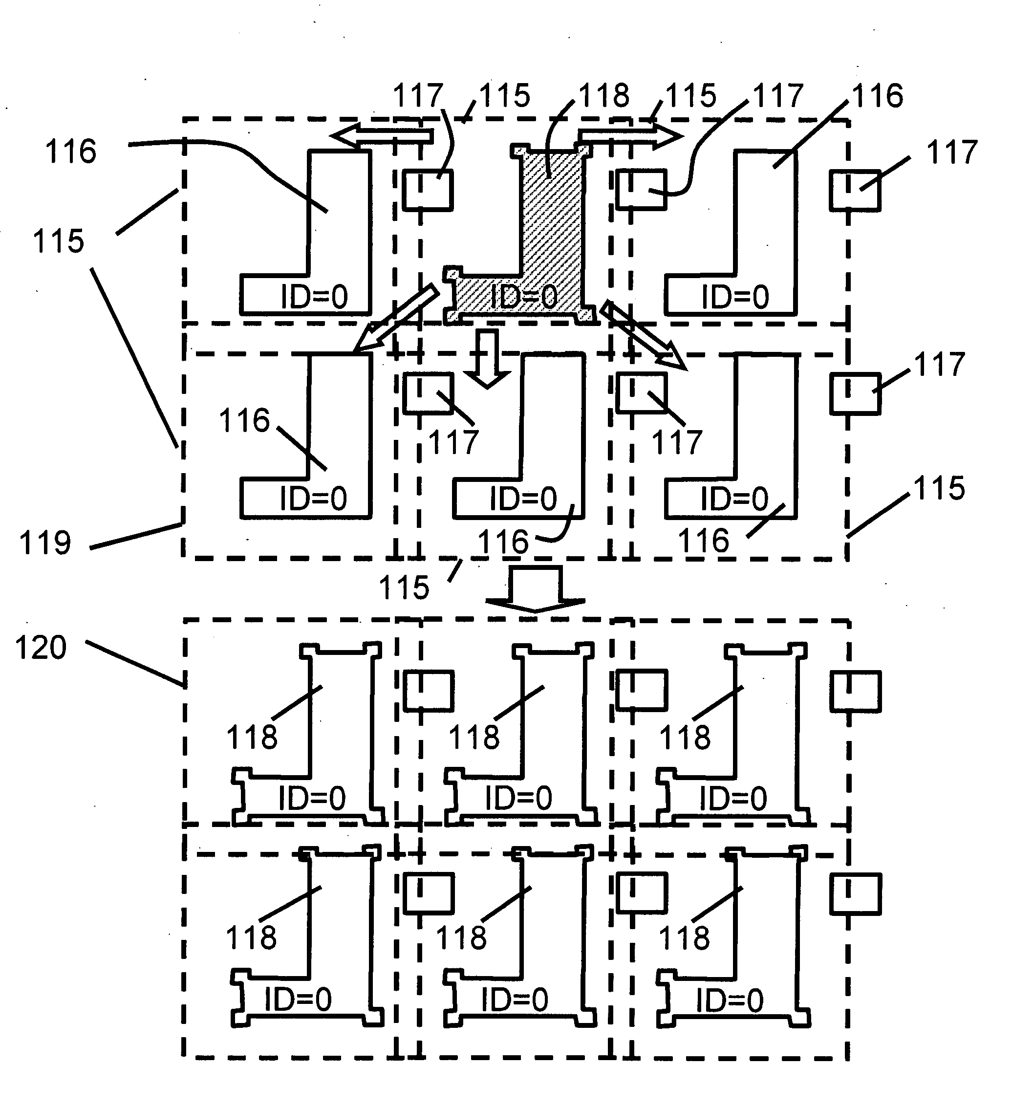
[0042]FIG. 1 is a flowchart showing the method for manufacturing a photomask according to the first embodiment. The method shown in FIG. 1 includes step 1: “reticle production starts”, step 2: “create design data”, step 3: “check design data”, step 4: “optical proximity effect correction”, ste...

second embodiment

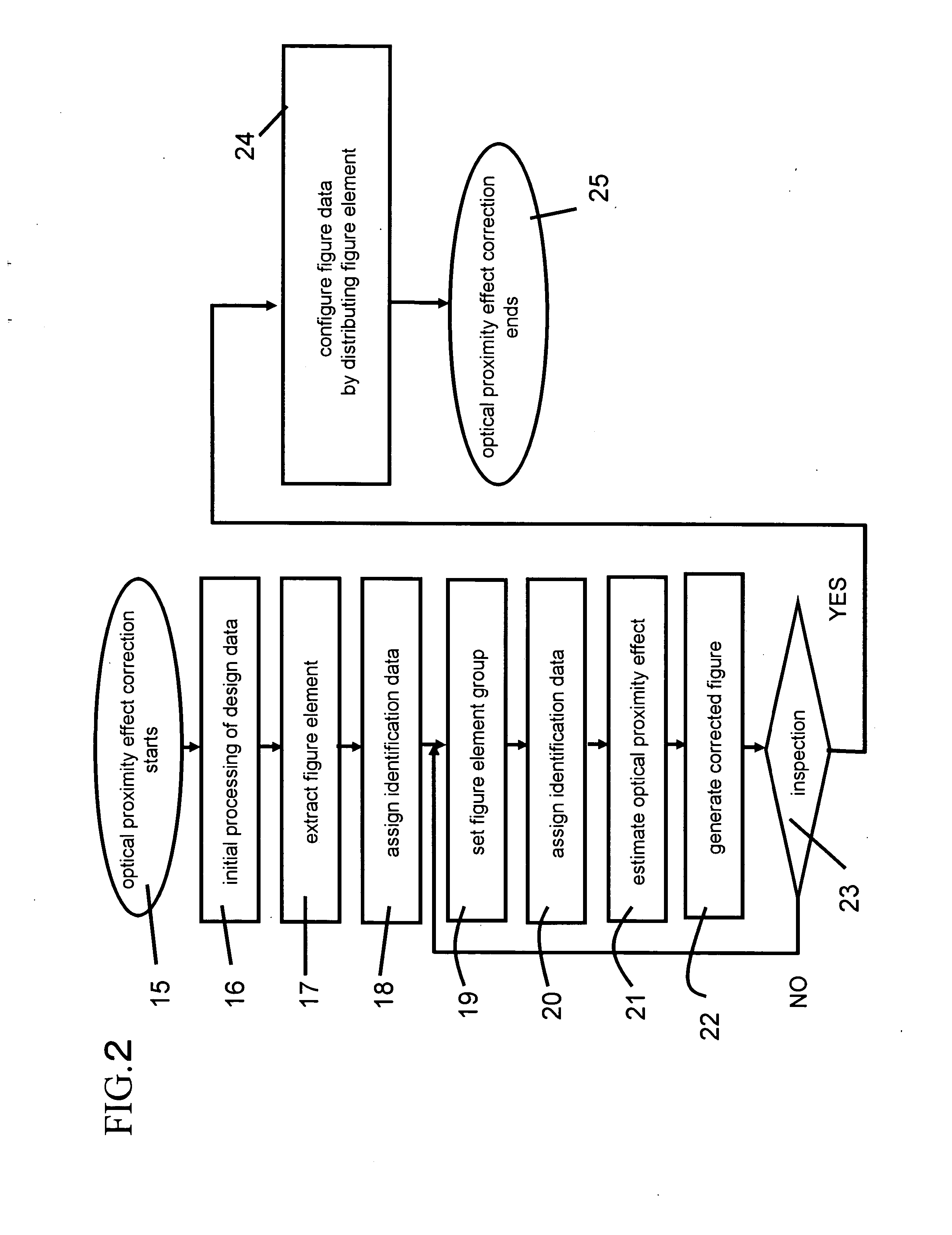
[0132] A method for manufacturing a photomask according to a second embodiment of the present invention has manufacturing processes similar to those in the method for manufacturing a photomask according to the first embodiment, except for optical proximity effect correction (step 4 in the flowchart shown in FIG. 1). An optical proximity effect correction process in the method for manufacturing a photomask according to the second embodiment will be described hereinbelow with reference to FIGS. 12 to 16.

[0133]FIG. 12 is a flowchart showing the details of the optical proximity effect correction process in the method for manufacturing a photomask according to the second embodiment. The process shown in FIG. 12 includes step 155: “optical proximity effect correction starts”, step 156: “initial processing of design data”, step 157: “extract figure-element sides”, step 158: “assign identification data”, step 159: “set group of figure-element sides”, step 160: “assign identification data”,...

third embodiment

[0163] A method for manufacturing a semiconductor device according to a third embodiment of the present invention using the reticle manufactured in the first or second embodiment will be described with reference to FIG. 17.

[0164]FIG. 17 is an illustration showing a process for forming a resist pattern on a semiconductor substrate using the reticle manufactured in the first or second embodiment, and a process for forming a metal wiring pattern on the semiconductor substrate by etching.

[0165] Referring to FIG. 17, the process for forming a resist pattern on a semiconductor substrate is performed by the following procedure: first, a metal layer 214 is deposited on a semiconductor substrate 215, and is coated with a resist 213. Then, a light 210 is applied to a reticle 211, and light transmitting the reticle 211 is focused by a projector lens 212 to expose the resist 213 to light. Layers 217 with the resist 213 exposed to light are shown in cross-section. Then, a resist 216 that is cu...


PUM


Abstract

A method for manufacturing a photomask based on design data includes the steps of forming a figure element group including a figure element in a layout pattern on the photomask and a figure element affecting the figure element due to the optical proximity effect, adding identical identification data to a data group indicating an identical figure element group, estimating an influence of the optical proximity effect on the figure element group, generating correction data indicating a corrected figure element in which the influence of the optical proximity effect is compensated for at the time of exposure, creating figure data by associating data having the identical identification data with correction data having the identical identification data, and forming a mask pattern on the photomask using figure data. Thus, the computation time for correction of the layout can be reduced, thereby reducing the production time of the photomask.

Description

CROSS-REFERENCE TO RELATED APPLICATIONS [0001] This application is based upon and claims the benefit of priority from the prior Japanese Patent Application No. 2005-099245, filed on Mar. 30, 2005, the entire contents of which are incorporated herein by reference. BACKGROUND OF THE INVENTION [0002] 1. Field of the Invention [0003] The present invention relates to a method for manufacturing a photomask, suitable for reducing the production time, and to a method for manufacturing a semiconductor device using the photomask. More specifically, the present invention relates to a method for manufacturing a photomask in which data for forming a pattern on the photomask can be created in a short time, and to a method for manufacturing a semiconductor device using the photomask. [0004] 2. Description of the Related Art [0005] With the recent reduction in size of semiconductor devices, there has been a demand for miniaturization of resist patterns formed by photolithography for manufacturing s...

Claims


Application Information

Patent Timeline
IPC IPC(8): G06F17/50G03F1/00G03C5/00G03F1/68G03F1/70H01L21/027
CPCG03F1/36G03F1/144G03F1/84G03F1/76
Inventor FUTATSUYA, HIROKIMORISHITA, KAZUMASA
Owner FUJITSU SEMICON LTD
Why Eureka
Try Eureka