Display device

a display device and display technology, applied in the field of display devices, can solve problems such as brightness due to brightness fluctuations, and achieve the effect of constant brightness and decreasing brightness changes

Inactive Publication Date: 2006-08-15
SEMICON ENERGY LAB CO LTD
View PDF35 Cites 22 Cited by
  • Summary
  • Abstract
  • Description
  • Claims
  • Application Information

AI Technical Summary

Benefits of technology

[0150]The above constitution makes it possible to provide a display device capable of emitting light maintaining nearly a constant brightness while decreasing a change in the brightness caused by a change in the current characteristics stemming from the deterioration in the EL elements.

Problems solved by technology

In the current-controlled type pixel, therefore, a problem arises concerning the dispersion in the brightness due to deterioration of the EL element.

Method used


Image

  • Display device
  • Display device
  • Display device

Examples


embodiment 1

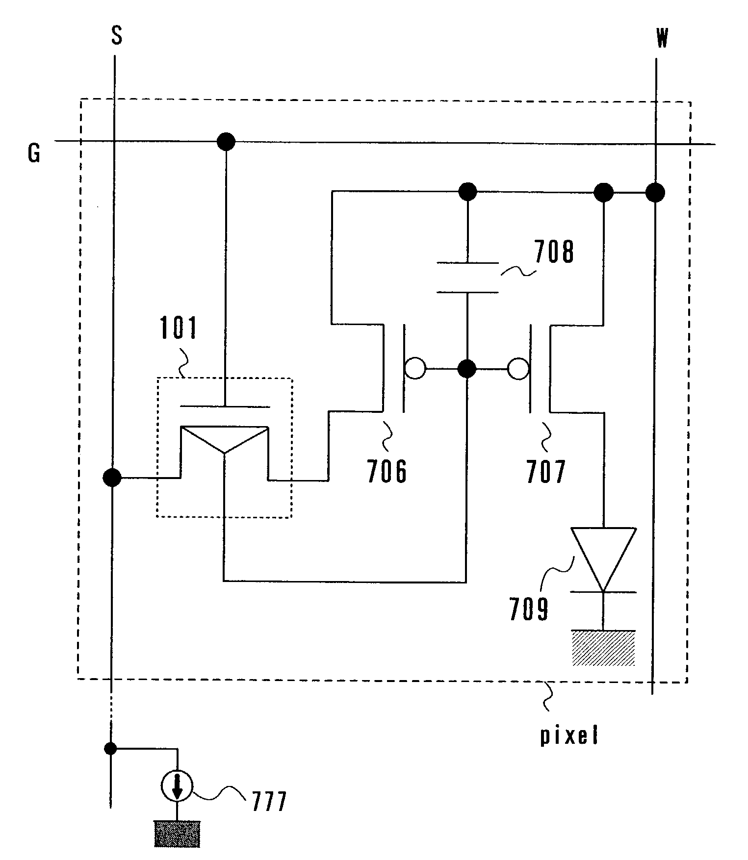
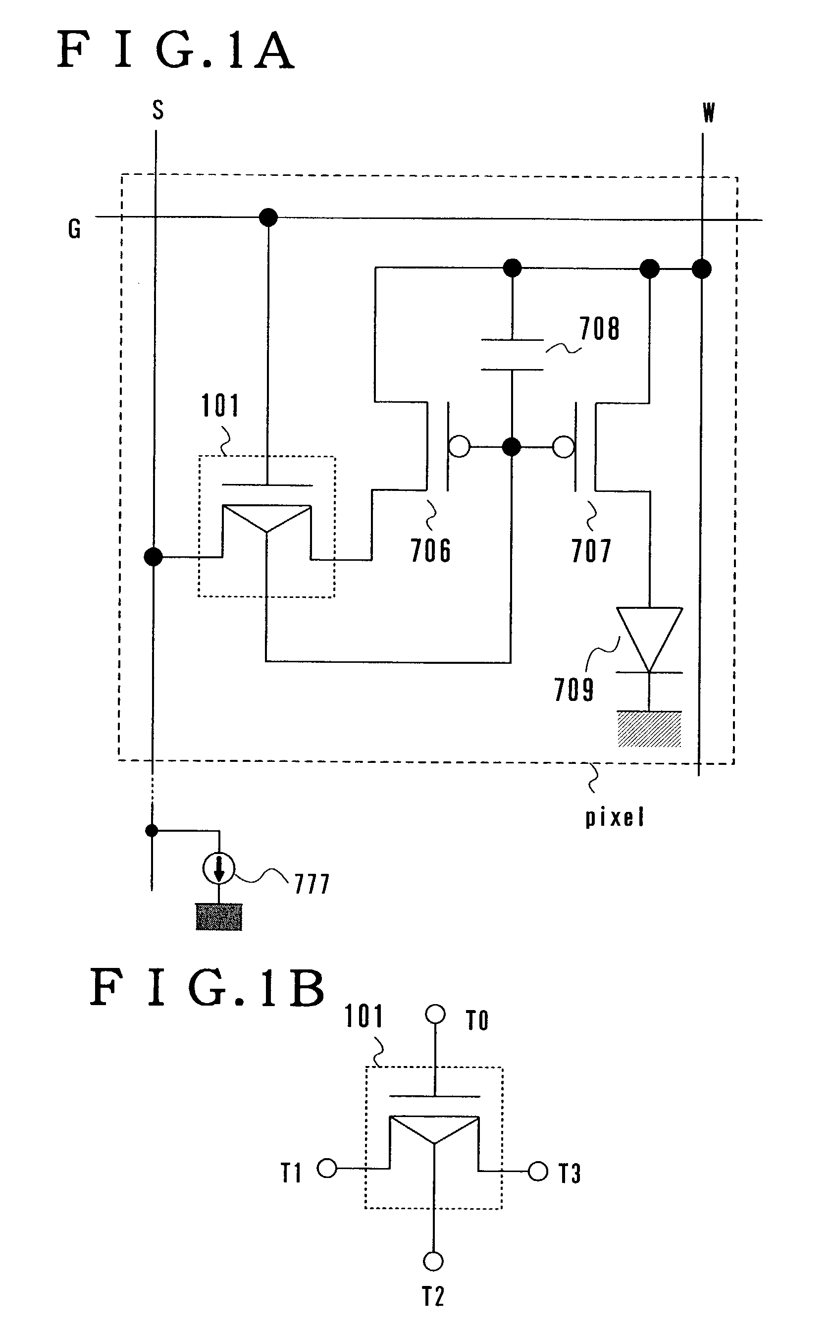
[0172]The embodiment 1 deals with the constitution of a multi-drain element and the constitution of a pixel in the display device of the invention using the multi-drain element. FIG. 1A illustrates the constitution of the pixel using the multi-drain element of the invention. In FIG. 1A, the portions same as those of the conventional pixel constitution shown in FIG. 10 are denoted by the same reference numerals but their description is not repeated. FIG. 1A illustrates a case where a drive TFT 707 and a current TFT 706 are the p-channel TFTs, and the pixel electrode is an anode.

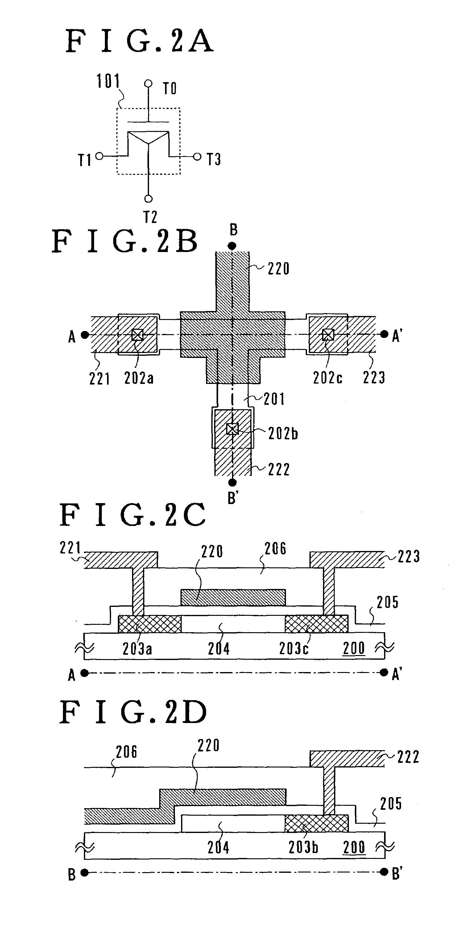
[0173]FIG. 1A employs a multi-drain element 101 instead of the select TFT 704 and holding TFT 705 used in FIG. 10. Terminals of the multi-drain element 101 in FIG. 1A will be described with reference to FIG. 1B. The multi-drain element 101 has a terminal T0 and terminals T1 to T3.

[0174]Depending upon a signal potential input to the terminal T0, the multi-drain element 101 selects a state where the terminals T1...

embodiment 2

[0213]The embodiment 2 deals with the pixel of a constitution different from that of the embodiment 1. FIG. 5 illustrates the constitution of the pixel of this embodiment. The portions same as those of FIGS. 1A–B are denoted by the same reference numerals but are not described here again. The pixel of the constitution shown in FIG. 5 is provided with an erasing TFT 501 in parallel with the holding capacitor 708. The erasing TFT 501 and the holding capacitor 708 need not necessarily be connected in parallel. When rendered conductive, the erasing TFT 501 may be so connected as to nearly equalize the potentials at both electrodes of the holding capacity 708. Owing to the above constitution, the electric charge held by the holding capacity 708 can be discharged by rendering the erasing TFT 501 conductive. Thus, the drive TFT 707 is rendered nonconductive. In the pixel in which the drive TFT 707 is rendered nonconductive, the EL element 709 does not emit light.

[0214]Here, the gate electr...

embodiment 3

[0233]This embodiment deals with the pixels of a constitution different from those of the pixels illustrated in the embodiments 1 and 2. FIGS. 8A and 8B illustrate the constitution of the pixel according to the embodiment 3. In FIGS. 8A and 8B, the same portions as those of FIGS. 1A–B and 5 are denoted by the same reference numerals, but their description is not repeated. In FIGS. 8A and 8B, the drive TFT 707 and the current TFT 706 in the pixel are the P-channel transistors, and the pixel electrode is an anode.

[0234]In FIGS. 8A and 8B, the first terminal of the current TFT 706, the gate electrode of the drive TFT 707 and the source signal line S are connected to one of different terminals T1 to T3 of the multi-drain element 101. Further, the first terminal of the current TFT 706 is connected to the gate electrode, and the second terminal of the current TFT 706 is connected to the power line W. The first terminal of the drive TFT 707 is connected to one electrode (anode) of the EL e...


PUM


Abstract

An EL display device free of a dispersion in the brightness caused by deterioration in the EL elements. The display device uses pixels of the current-controlled type to suppress a change in the current flowing through the EL elements caused by the deterioration in the EL elements. The display device further uses elements capable of short-circuiting or opening three nodes simultaneously. No bank is used for dividing the EL layers into separate colors. EL elements of the mixed junction type are used. A reverse bias voltage is applied to the EL elements at regular intervals. The display device suppresses dispersion in the brightness caused by the deterioration in the EL elements.

Description

BACKGROUND OF THE INVENTION[0001]1. Field of the Invention[0002]The present invention relates to a display device in which a light-emitting element is provided in each of the pixels. In particular, the invention relates to a display device of the active matrix type in which a transistor is provided for each of the pixels to control the emission of light from the light-emitting elements. The invention further relates to electronic devices using the display device.[0003]2. Description of the Related Art[0004]There has been proposed a display device of the active matrix type in which a light-emitting element and a transistor are arranged for each of the pixels to control the emission of light from the light-emitting element. In particular, attention has been given to the display device of the active matrix type using thin-film transistors (hereinafter referred to as TFTs) as transistors.[0005]The light-emitting element has a first electrode and a second electrode, and changes its brigh...

Claims


Application Information

Patent Timeline
Patent Type & Authority Patents(United States)
IPC IPC(8): G09G3/30G09G3/32G09F9/30H01L51/50G09G3/20H05B44/00H01L27/32H01L29/786
CPCG09G3/3241G09G3/2022G09G3/2029G09G2300/0426G09G2300/0809G09G2330/08G09G2300/0852G09G2310/0256G09G2320/0233G09G2320/043G09G2300/0842
Inventor INUKAI, KAZUTAKASEO, SATOSHIYAMAZAKI, SHUNPEI
Owner SEMICON ENERGY LAB CO LTD
Why Eureka
Try Eureka