Circuit and method for lowering insertion loss and increasing bandwidth in MOSFET switches

a technology of mosfet switches and insertion losses, which is applied in the field of mosfet devices, can solve the problems of reducing the bandwidth and increasing the resistance of the switch, and achieve the effects of increasing the bandwidth of the switch, and reducing the insertion loss

Active Publication Date: 2006-08-22
SEMICON COMPONENTS IND LLC
View PDF7 Cites 48 Cited by
  • Summary
  • Abstract
  • Description
  • Claims
  • Application Information

AI Technical Summary

Benefits of technology

[0011]In view of the foregoing background discussion, the present invention provides a symmetric DC coupled primary FET switch. The input signal may be connected to either the source or the drain of the FET switch with an output from the drain or the source, respectively. Two other FET switches are provided, one connects the well of the primary FET switch to its source and the second connects the well to its drain. The gates of the primary FET switch and the two other FET switches are driven in concert by an enable signal. All three are on or off together. The function of the two other FET switches drive the well of the primary FET with the same signal that appears at the input and the output. This action substantially reduces the loss of the input signal with frequency through the source-well (Csw) and the drain-well (Cdw) capacitors. The net effect is to reduce the insertion loss at higher frequencies and increase the bandwidth of the switch.
[0012]When the enable is false the primary FET switch and the other two FET switches are turned off, and a fourth FET switch is on connecting the well of the first three FET's to a suitable potential. The potential is low when the first three FET's are n-types and high when they are p-types. The operation of this fourth FET improves the off-isolation of the switch.
[0013]Input signal is lost via the source-gate (Csg) and the drain-gate (Cdg) capacitors to the gate of the primary FET switch. To reduce this loss a resistor is placed between the enable signal and the gate of the primary FET switch. The resistor increases the break frequency of this resistor / capacitor circuit. This reduces the insertion loss at higher frequencies and increases the bandwidth of the primary FET switch. The resistor may be bypassed to decrease the turn off time.

Problems solved by technology

That is, the switch on-resistance increases which, in turn, reduces its bandwidth.

Method used


Image

  • Circuit and method for lowering insertion loss and increasing bandwidth in MOSFET switches
  • Circuit and method for lowering insertion loss and increasing bandwidth in MOSFET switches
  • Circuit and method for lowering insertion loss and increasing bandwidth in MOSFET switches

Examples


Embodiment Construction

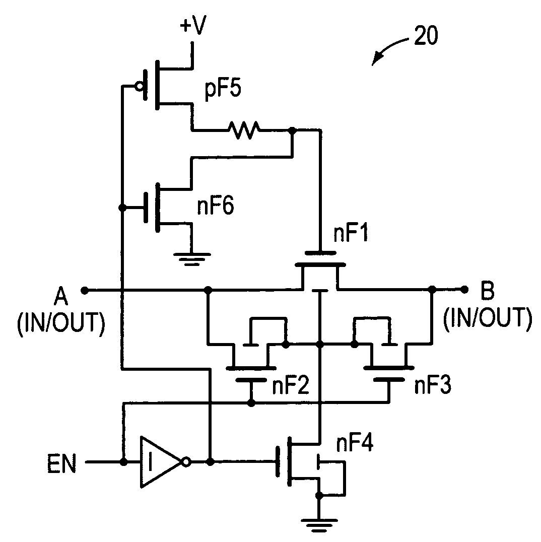
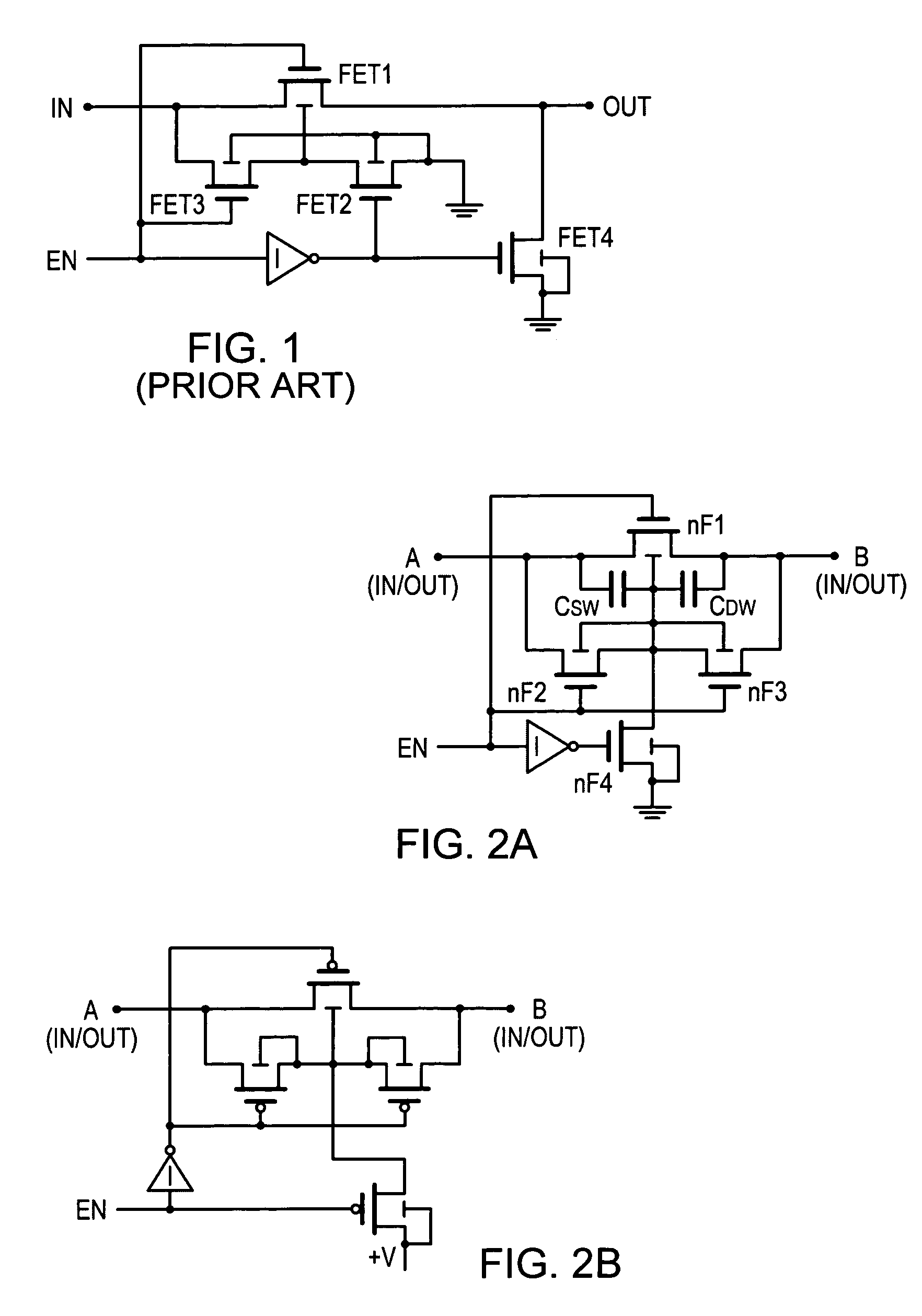
[0024]FIG. 2A is an embodiment of the present invention where an input signal may be introduced at node A or B emerging at node B or A, respectively, when the switch nF1 is on. In this circuit there is an n-type MOSFET nF2 with common source, gate and well connections as with nF1. There is also an n-type MOSFET, nF3, with common drain, gate, and well connection as with nF1. The drain of nF2 is connected to the source of nF3 and the well of nF1. The n-type MOSFET's in the embodiments of the present invention are constructed with their p-wells isolated from the p-substrate, usually by an n-type well. This type of construction is well known in the art.

[0025]With n-type MOSFETs, EN high turns on nF1, nF2 and nF3. In practice nF2 and nF3 are made the same size, and thus the basic switch is bilateral offering the same impedance in either direction. When EN is low, the circuit also offers the same high impedance in either direction when nF1, nF2 and nF3 are all off, and nF4 is on driving t...


PUM


Abstract

A DC symmetrical FET switch includes second and third switches connecting the well of the symmetrical FET switch to the drains and the source when the symmetrical FET switch is on. When the three FET's are on, the well, source and drain of the symmetric FET switch all exhibit the same input signal, wherein the drains and source to well capacitances are substantially prevented from draining off any of the input signal, thereby increasing the bandwidth and decreasing the insertion loss of the switch. The second and third switches are also FET switches. An enable signal is connected to the gates of all three FET's turning them on and off together. When the enable is false the FET switches are turned off and their wells are driven to a potential a proper potential. When the FET's are n-type the potential is low and when the FET's are p-types the potential is high. A resistor is provided in the gate drive of the first FET switch that further increases bandwidth and decreases insertion loss of the switch by moving the break frequency of the drain and source to gate capacitances.

Description

BACKGROUND OF THE INVENTION[0001]1. Field of the Invention[0002]The present invention relates to MOSFET devices and more particularly to MOSFET devices used as low on-impedance switches.[0003]2. Background Information[0004]MOSFET switches are found in many applications and have become common in high frequency switch applications. Known designs have focused on lowering insertion loss and increasing the bandwidth by minimizing the “body effect,” that is inherent in MOSFET structures. Insertion loss can be described, generally, as the loss of signal power delivered to a load due to the addition of a less than perfect switch compared to that if the switch were perfect.[0005]The body effect becomes significant when the FET switch is turned on and neither the source nor the drain are at the same potential as the well. In such instances, the well acts like another gate (sometimes referred to as a “back gate”) and produces a localized increase in the threshold voltage of the device which in...

Claims


Application Information

Patent Timeline
Patent Type & Authority Patents(United States)
IPC IPC(8): H03K17/687
CPCH03K17/162H03K17/6871H03K2217/0018
Inventor MISKE, MYRON J.
Owner SEMICON COMPONENTS IND LLC
Why Eureka
Try Eureka