Semiconductor integrated circuit having functional modules each including a built-in self testing circuit

a technology of integrated circuits and functional modules, applied in the field of semiconductor integrated circuits, can solve the problems of reducing the scale of the system configuration, including the power-on detection circuit provided outside the lsi, and the accuracy of the self-test less than completely reliable, so as to reduce the physical size of the nonvolatile memories

Active Publication Date: 2006-08-22
LAPIS SEMICON CO LTD
View PDF6 Cites 24 Cited by
  • Summary
  • Abstract
  • Description
  • Claims
  • Application Information

AI Technical Summary

Benefits of technology

[0007]The main object of the present invention, which has been completed by addressing the problems of semiconductor integrated circuits in the related art discussed above, is to provide a new and improved semiconductor integrated circuit that allows a self test in the semiconductor integrated circuit which is built in a system to be conducted through a circuit structure on a smaller scale and achieves an improvement in the accuracy of the self test.
[0009]This structure, which includes built-in self testing circuits provided for the individual functional modules and thus does not require any external components, enables an automatic self test to be conducted inside the semiconductor integrated circuit. The structure allows the scale of the system, which includes the semiconductor integrated circuit, to be reduced. In addition, by building up the built-in self testing circuits at the individual functional modules to a sufficient degree, a self test can be conducted that is comparable to the quality of factory tests conducted prior to shipment, even after the semiconductor integrated circuit is mounted in the system.
[0010]Furthermore, the semiconductor integrated circuit may include a power-on detection circuit (103) that detects that the power has been turned on. Since this allows the semiconductor integrated circuit to detect that the power to the semiconductor integrated circuit has been turned on for itself, the semiconductor integrated circuit can automatically shift into a self test mode. In addition, since the power-on detection circuit is built into the semiconductor integrated circuit instead of providing it as an external component, the scale of the system having the built-in semiconductor integrated circuit can be reduced.
[0012]By providing a switch (110a) for disconnecting the functional modules from an input / output terminal (110) during a self test of the functional modules, the individual functional modules can be prevented from becoming affected by any external factors originating from the outside of the semiconductor integrated circuit during the self test.
[0013]By providing at each functional module a self test result output terminal (208) through which the results of the self test are to be output, the length of time required to analyze any problems is reduced to achieve quick feedback.
[0014]In addition, by providing a counter (207) capable of measuring the length of time elapsing through a self test and outputting a time count together with the results of the self test, information is provided indicating specifically at what point in time during the self test cycle a given problem is discovered in each self test to make it possible to identify a problem even more accurately.

Problems solved by technology

Some LSIs, such as system LSIs (large-scale integrated circuits) mounted in vehicles, are utilized under difficult conditions such as high temperature or vibration.
However, the following problems arise in the self testing method described above.
Firstly, the scale of the system configuration, which includes a power-on detection circuit provided outside the LSI, is bound to be large.
In such a case, the presence of the test ROM itself poses an obstacle to reducing the scale of the system LSI.
Secondly, since the internal operation at the LSI is executed via a CPU (central processing unit), only part of the LSI can be tested, making the accuracy of the self test less than completely reliable.

Method used


Image

  • Semiconductor integrated circuit having functional modules each including a built-in self testing circuit
  • Semiconductor integrated circuit having functional modules each including a built-in self testing circuit
  • Semiconductor integrated circuit having functional modules each including a built-in self testing circuit

Examples


first embodiment

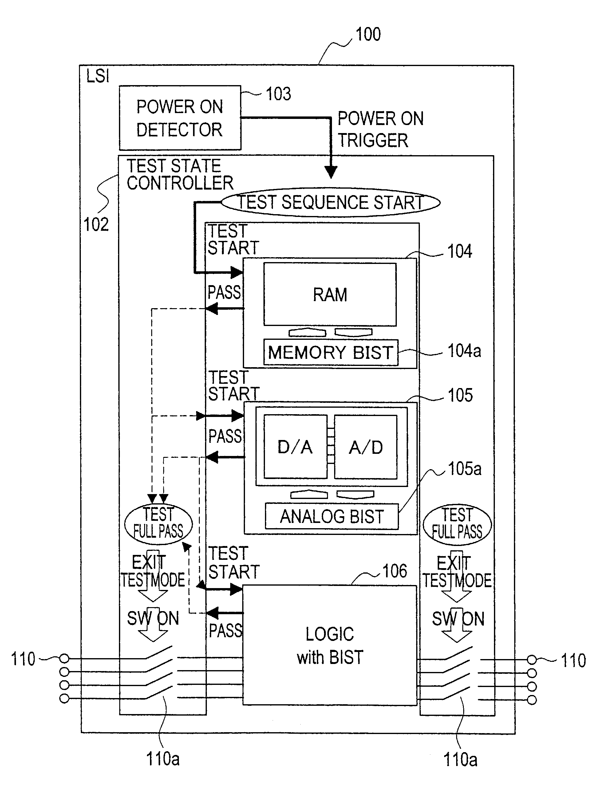
[0024]The semiconductor integrated circuit in the first embodiment is now explained in reference to FIG. 1.

[0025]A semiconductor integrated circuit 100 comprises a power-on detection circuit 103 that detects that the power to the semiconductor integrated circuit 100 has been turned on and a self test control circuit 102 that shifts the semiconductor integrated circuit 100 into a self test mode in response to a trigger signal generated by the power-on detection circuit 103.

[0026]A memory 104, an analog circuit 105 and a logic circuit 106 each constituted as a functional module are mounted at the semiconductor integrated circuit 100. The memory 104 in this structure may be, for instance, a RAM (random access memory) which is a volatile storage medium. The RAM may be any of various types of RAM including DRAM (dynamic RAM) having a dynamic storage function. In addition, the analog circuit 105 may be, for instance, a digital / analog (D / A) converter or an analog / digital (A / D) converter.

[0...

second embodiment

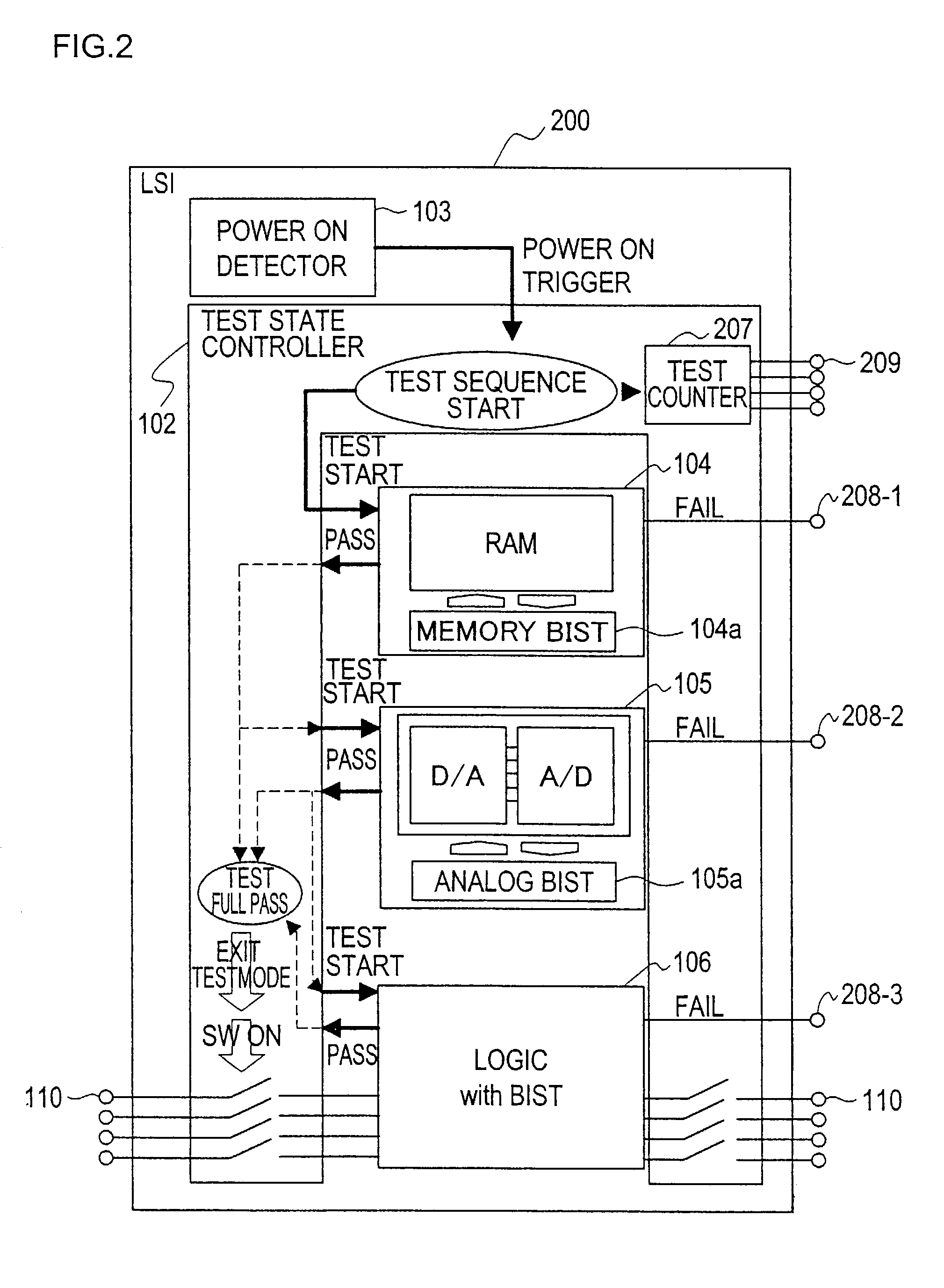
[0037]The semiconductor integrated circuit in the second embodiment is now explained in reference to FIG. 2.

[0038]As shown in FIG. 2, a semiconductor integrated circuit 200 is achieved by adding self test result output terminals 208-1, 208-2 and 208-3 through which the results of the self tests are output to the outside, a test counter 208 capable of measuring the length of time (test cycle) elapsing through each self test to allow information as to at what point in time an error has occurred to be output and a counter output terminal 209 through which the value obtained at the test counter 207 is output to the structure of the semiconductor integrated circuit 100 achieved in the first embodiment. Since other components are substantially identical to those in the first embodiment, the same reference numerals are assigned to them to preclude the necessity for a repeated explanation thereof.

[0039]Next, the individual self testing operations performed on the memory 104, the analog circ...

third embodiment

[0043]An example of the logic circuit 106 and an example of the logic built-in self testing circuit provided in part of the logic circuit are now explained in reference to the third embodiment.

[0044]FIG. 3 shows an example of a logic circuit having a SCAN test circuit.

[0045]This logic circuit 300 includes a testing system for conducting a test referred to as a SCAN test. The logic circuit 300 may be tested at the time of shipment of the product in which the logic circuit 300 is mounted, for instance. In the test mode, the chip terminals of the logic circuit 300 are designated as a SCAN shift enable terminal 301, SCAN-in terminals 302-1 and 302-2, SCAN-out terminals 303-1 and 303-2, a clock terminal 304 and a SCAN test mode terminal 305. The designations of the individual terminals are determined by terminal designation selectors 310-1 and 310-2.

[0046]Next, the testing operation performed in the logic circuit 300 is explained.

[0047]The test is started as a test mode signal is input t...


PUM


Abstract

A semiconductor integrated circuit that allows a self test of an integrated circuit built into a system to be conducted through a circuit structure on a smaller scale and achieves an improvement in the accuracy of the self test is provided. An integrated circuit includes functional modules respectively provided with built-in self testing circuits and a self test control circuit that individually controls the built-in self testing circuits. This structure allows self tests to be automatically performed within the integrated circuit without requiring external components. The scale of the system having the built-in integrated circuit may thus be reduced. Also, by building up the built-in self testing circuits in the individual functional modules to a sufficient degree, a high-quality self test comparable to that conducted prior to shipment can be performed even after the integrated circuit is built into the system.

Description

BACKGROUND OF THE INVENTION[0001]1. Field of the Invention[0002]The present invention relates to a semiconductor integrated circuit, and more specifically, it relates to a semiconductor integrated circuit having a built-in self test: (BIST) system.[0003]2. Description of the Related Art[0004]Some LSIs, such as system LSIs (large-scale integrated circuits) mounted in vehicles, are utilized under difficult conditions such as high temperature or vibration. When an LSI is used under such conditions, the LSI must be tested in some way even after the LSI is installed in the product in order to ensure that the LSI is not engaged in operation after a failure occurs therein. Under normal circumstances, the LSI conducts a self test every time power to the product is turned on.[0005]A test ROM (read only memory) having a test program written therein is normally mounted outside the LSI to enable the LSI to conduct the self test. The operation of the LSI is tested in conformance to the test prog...

Claims


Application Information

Patent Timeline
Patent Type & Authority Patents(United States)
IPC IPC(8): G06F11/00G01R31/3167G01R31/317G01R31/3185G11C29/14
CPCG01R31/31724G11C29/14G01R31/3167G01R31/31701G11C2029/3202G11C2029/0407G01R31/318533
Inventor OZAWA, KAZUMASA
Owner LAPIS SEMICON CO LTD
Why Eureka
Try Eureka