Nonvolatile flash memory and method of operating the same

a nonvolatile memory and flash memory technology, applied in the direction of digital storage, semiconductor devices, instruments, etc., can solve the problems of increasing cost, reducing yield, reducing current requirements, etc., and achieve the effect of reducing current requirements and improving current flow efficiency

Active Publication Date: 2006-08-29
YIELD MICROELECTRONICS CORP
View PDF10 Cites 81 Cited by
  • Summary
  • Abstract
  • Description
  • Claims
  • Application Information

AI Technical Summary

Benefits of technology

[0007]An object of the present invention is to provide a nonvolatile memory cell structure and a method of operating the same, wherein a single floating gate is used. When performing a program step, a nontrivial voltage is applied to the source or a back bias is applied to the transistor substrate to form a wider and depleted source / substrate junction, thereby improving the efficiency of current flowing to the floating gate and thus greatly reducing the current requirement of performing a program step to a single gate EEPROM.
[0009]Another object of the present invention is to provide a nonvolatile memory cell to accomplish the effects of a low operation current, high reliability and also miniaturize the size of the whole memory chip.

Problems solved by technology

As compared to the common CMOS fabrication process, there are more steps of film deposition, etch, and photolithography, hence increasing the cost, complicating the process, lowering the yield and lengthening the fabrication time.
This structure, however, has the problems of low reliability, interference from non-selected memory cells during the program step, and over erase. FIG. 1 shows a conventional EEPROM memory cell structure.
Therefore, for the conventional single-gate EEPROM, the whole operation current can't be reduced easily.
Moreover, because the memory cell array becomes denser and denser, the channel length shortens accordingly, hence causing mutual interference between memory cells.
Furthermore, a complicated peripheral circuit design is required for a higher operation current.
Therefore, the above high-voltage operation method will increase the complexity of the peripheral circuit.
Because the structure of a single-gate EEPROM memory cell is a sandwich structure of transistor substrate-floating gate-capacitor substrate, stored electric charges can be released to either direction according to the direction of the applied electric field, hence more deteriorating the problem of over erase of the single-gate EEPROM.

Method used


Image

  • Nonvolatile flash memory and method of operating the same
  • Nonvolatile flash memory and method of operating the same
  • Nonvolatile flash memory and method of operating the same

Examples


Embodiment Construction

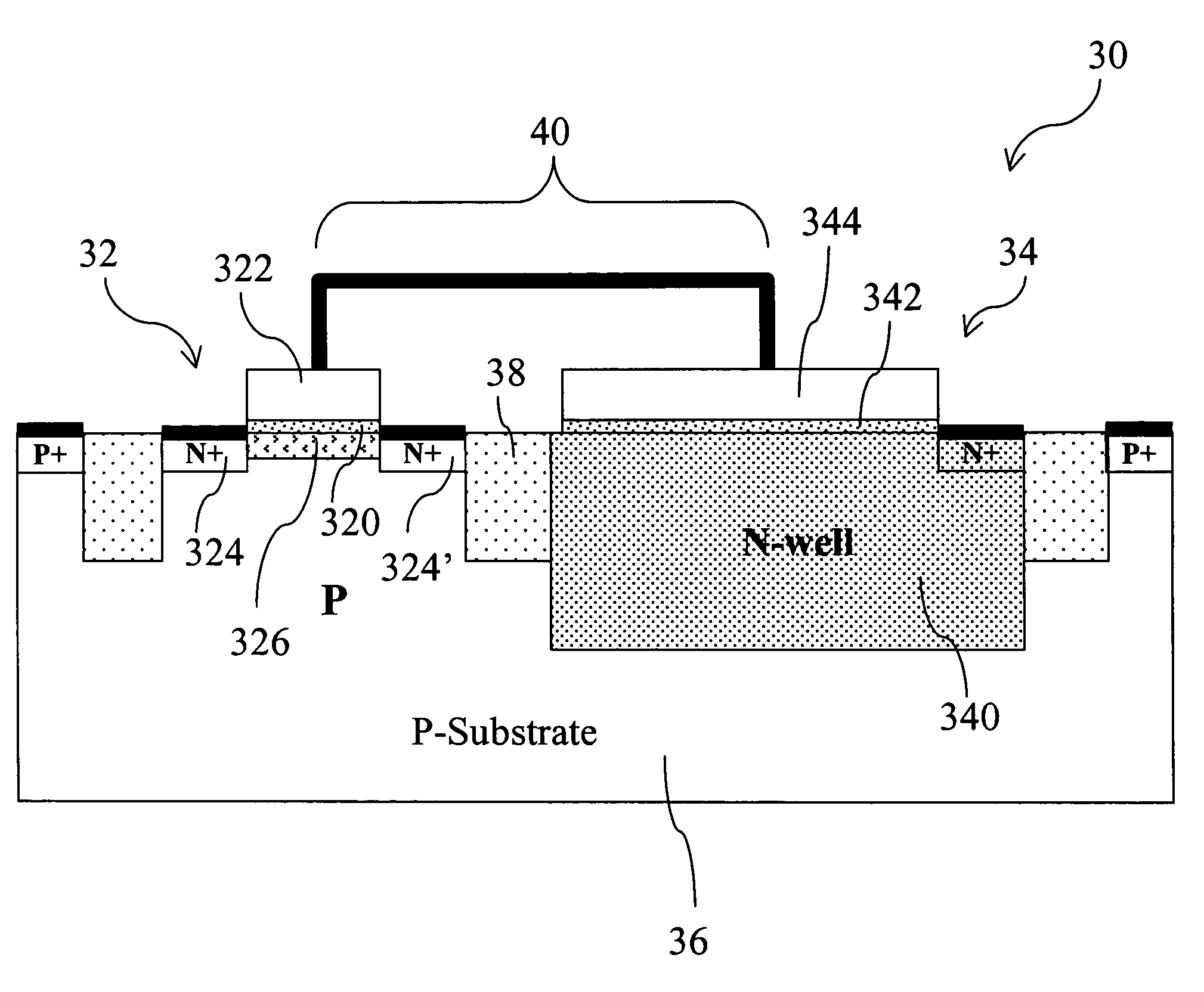
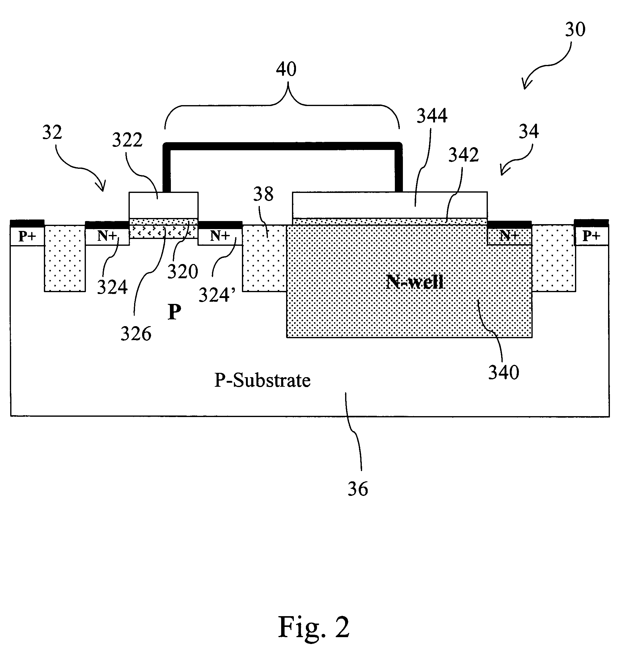
[0025]As shown in FIG. 2, a single-gate EEPROM memory cell 30 comprises an NMOS transistor (NMOSFET) 32 and an N-well capacitor 34 in a p-type silicon substrate 36. The NMOSFET 32 comprises a first dielectric 320 on the surface of the p-type silicon substrate 36, a first conducting gate 322 stacked above the first dielectric 320 and two n+ doped regions in the p-type silicon substrate 36 as a source 324 and a drain 324′. A channel 326 is formed between the source 324 and the drain 324′. The N-well capacitor 34 comprises a doped region in the p-type silicon substrate 36 (i.e., an N-well 340), a second dielectric 342 on the surface of the N-well 340, and a second conducting gate 344 stacked above the second dielectric 342 to form a sandwich capacitor structure of top plate-dielectric-bottom plate. The conducting gate 322 of the NMOSFET 32 and the conducting gate 344 of the N-well capacitor 34 are electrically connected together and isolated by an isolator 38 to form the structure of a...


PUM


Abstract

A nonvolatile memory and a method of operating the same are proposed. The nonvolatile memory has single-gate memory cells, wherein a structure of a transistor and a capacitor is embedded in a semiconductor substrate. The transistor comprises a first conducting gate stacked on the surface of a dielectric with doped regions formed at two sides thereof as a source and a drain. The capacitor comprises a doped region, a dielectric stacked thereon, and a second conducting gate. The conducting gates of the capacitor and the transistor are electrically connected together to form a single floating gate of the memory cell. The semiconductor substrate is p-type or n-type. Besides, a back-bias program write-in and related erase and readout operation ways are proposed for the single-gate memory cells.

Description

FIELD OF THE INVENTION[0001]The present invention relates to the structure of a nonvolatile memory and, more particularly, to the structure of a flash memory with an ultra-low program current and a high-homogeneity erase architecture and a method of operating the same.BACKGROUND OF THE INVENTION[0002]The complementary metal oxide semiconductor (CMOS) fabrication technology has become a common fabrication method of application specific integrated circuits (ASIC). Today, electrically erasable programmable read only memories (EEPROM) have been widely used in electronic products because of their non-volatile functions of electrically writing and erasing data.[0003]Nonvolatile memory cells are programmable. Electric charges are stored to change the gate voltages of memory cell transistors, or electric charges are not stored to keep the original gate voltages of memory cell transistors. The erase operation removes all electric charges stored in nonvolatile memory cells to let all nonvolat...

Claims


Application Information

Patent Timeline
Patent Type & Authority Patents(United States)
IPC IPC(8): G11C16/04G11C11/34
CPCG11C16/0416G11C16/3477G11C2216/10
Inventor WANG, LEE ZHUNGHUANG, DANIELLIN, HSIN CHANGCHANG, ROGET
Owner YIELD MICROELECTRONICS CORP
Why Eureka
Try Eureka