

Page buffer for flash memory device
a flash memory device and buffer technology, applied in digital storage, buildings, instruments, etc., can solve problems such as program errors
- Summary
- Abstract
- Description
- Claims
- Application Information
AI Technical Summary
Benefits of technology
Problems solved by technology
Method used
Image

Examples
Embodiment Construction
[0012]Preferred embodiments of the present invention will be described below in more detail with reference to the accompanying drawings. The present invention may, however, be embodied in different forms and should not be constructed as limited to the embodiments set forth herein. Rather, these embodiments are provided so that this disclosure will be thorough and complete, and will fully convey the scope of the invention to those skilled in the art. Like numerals refer to like elements throughout the specification.
[0013]Hereinafter, it will be described about an exemplary embodiment of the present invention in conjunction with the accompanying drawings.
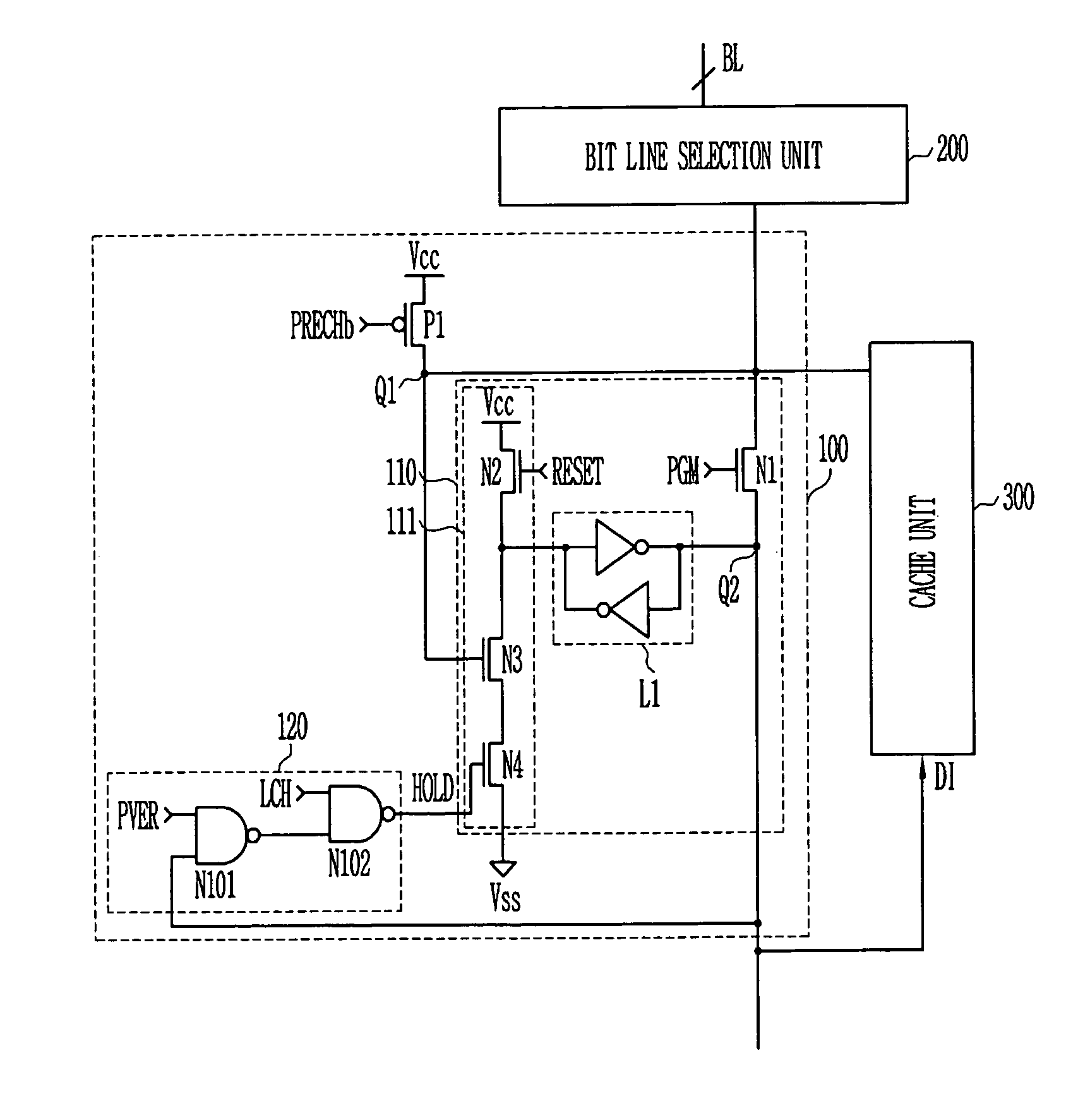
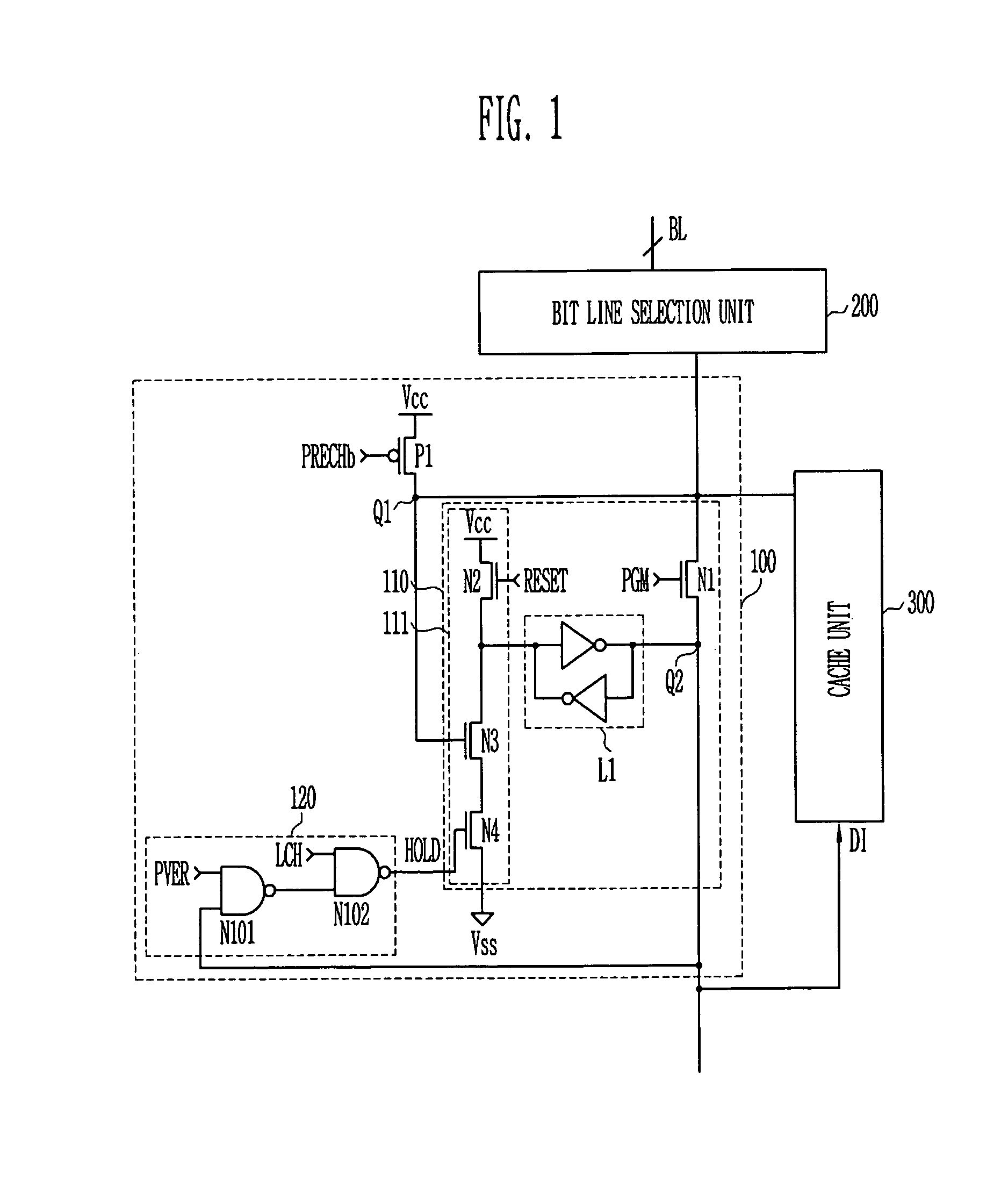
[0014]FIG. 1 shows a page buffer of a flash memory device of the present invention.
[0015]Referring to FIG. 1, the flash memory device according to the present invention includes a page buffer 100, a bit line selection unit 200, and a cache unit 300. The page buffer 100 senses and latches data of a flash memory cell. The bit line selec...
PUM
 Abstract
Description
Claims
Application Information