In-line voltage contrast determination of tunnel oxide weakness in integrated circuit technology development

Inactive Publication Date: 2006-09-05
ADVANCED MICRO DEVICES INC
View PDF7 Cites 83 Cited by
  • Summary
  • Abstract
  • Description
  • Claims
  • Application Information

AI Technical Summary

Problems solved by technology

Integrated circuits are made in and on silicon wafers by extremely complex systems that require the coordination of hundreds or even thousands of precisely controlled processes to produce a finished semiconductor wafer.
A 100% yield is extremely difficult to obtain because minor variations, due to such factors as timing, temperature, and materials, substantially affect a process.
Further, one process often affects a number of other processes, often in unpredictable ways.
Major variations in the processes are not possible because of the time and cost of using production equipment and production wafers.
Unf

Method used


Image

  • In-line voltage contrast determination of tunnel oxide weakness in integrated circuit technology development
  • In-line voltage contrast determination of tunnel oxide weakness in integrated circuit technology development
  • In-line voltage contrast determination of tunnel oxide weakness in integrated circuit technology development

Examples


Embodiment Construction

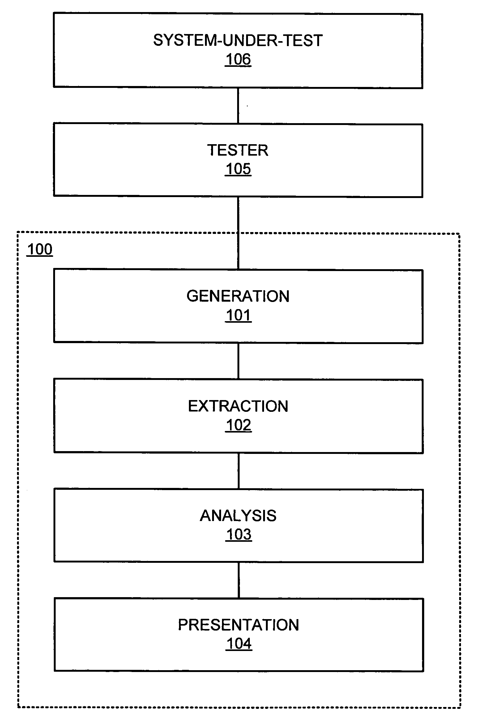
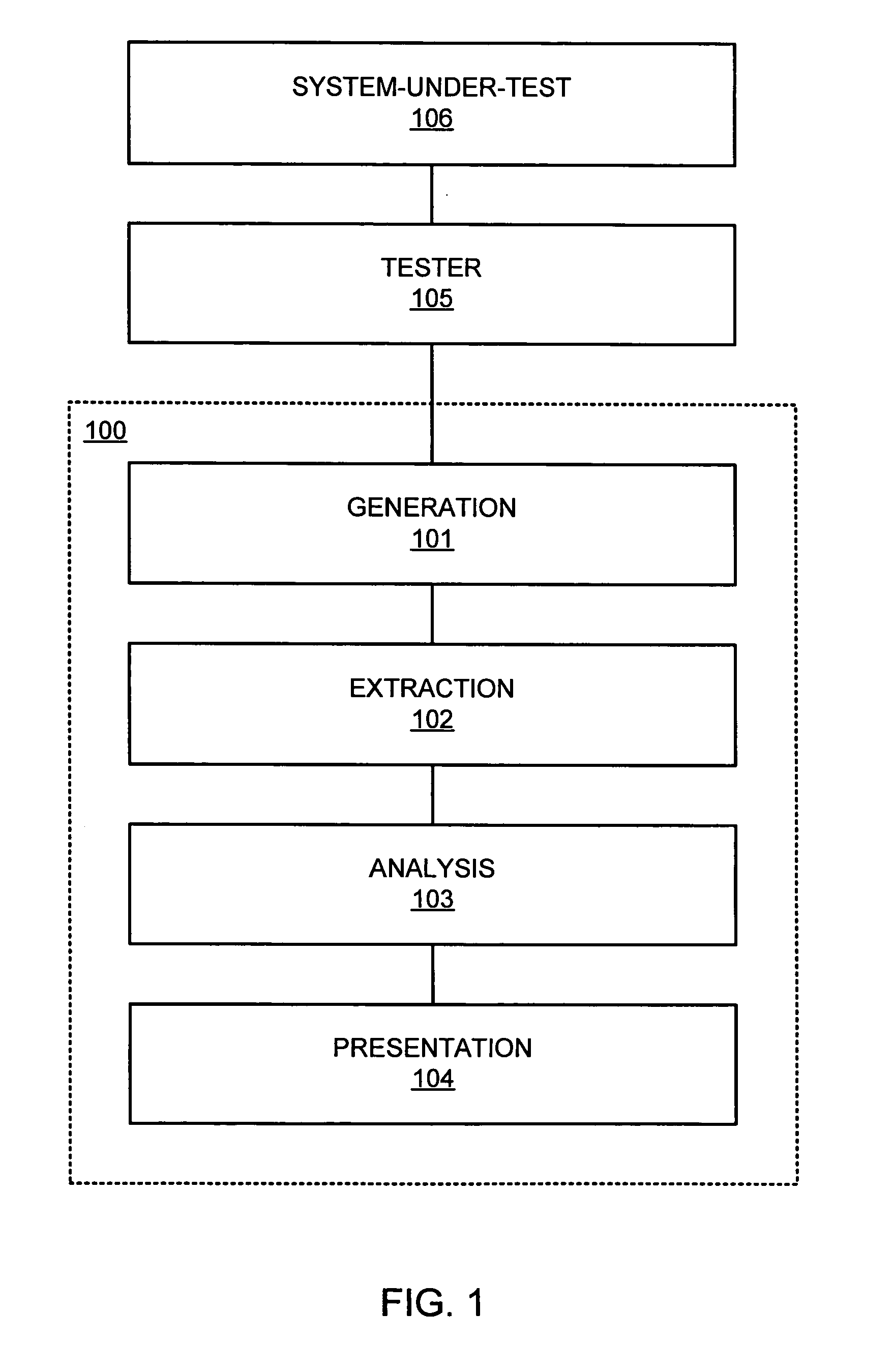
[0021]In the following description, numerous specific details are given to provide a thorough understanding of the invention. However, it will be apparent that the invention may be practiced without these specific details. In order to avoid obscuring the present invention, some well-known process steps are not disclosed in detail. Likewise, the drawings showing embodiments of the device are semi-diagrammatic and not to scale and, particularly, some of the dimensions are for the clarity of presentation and are shown exaggerated in the FIGs. The same numbers are used in the drawing FIGs. to relate to the same elements.

[0022]The term “horizontal” as used herein is defined as a plane parallel to a substrate or wafer. The term “vertical” refers to a direction perpendicular to the horizontal as just defined. Terms, such as “on”, “above”, “below”, “bottom”, “top”, “side” (as in “sidewall”), “higher”, “lower”, “over”, and “under”, are defined with respect to the horizontal plane. The term “...


PUM


Abstract

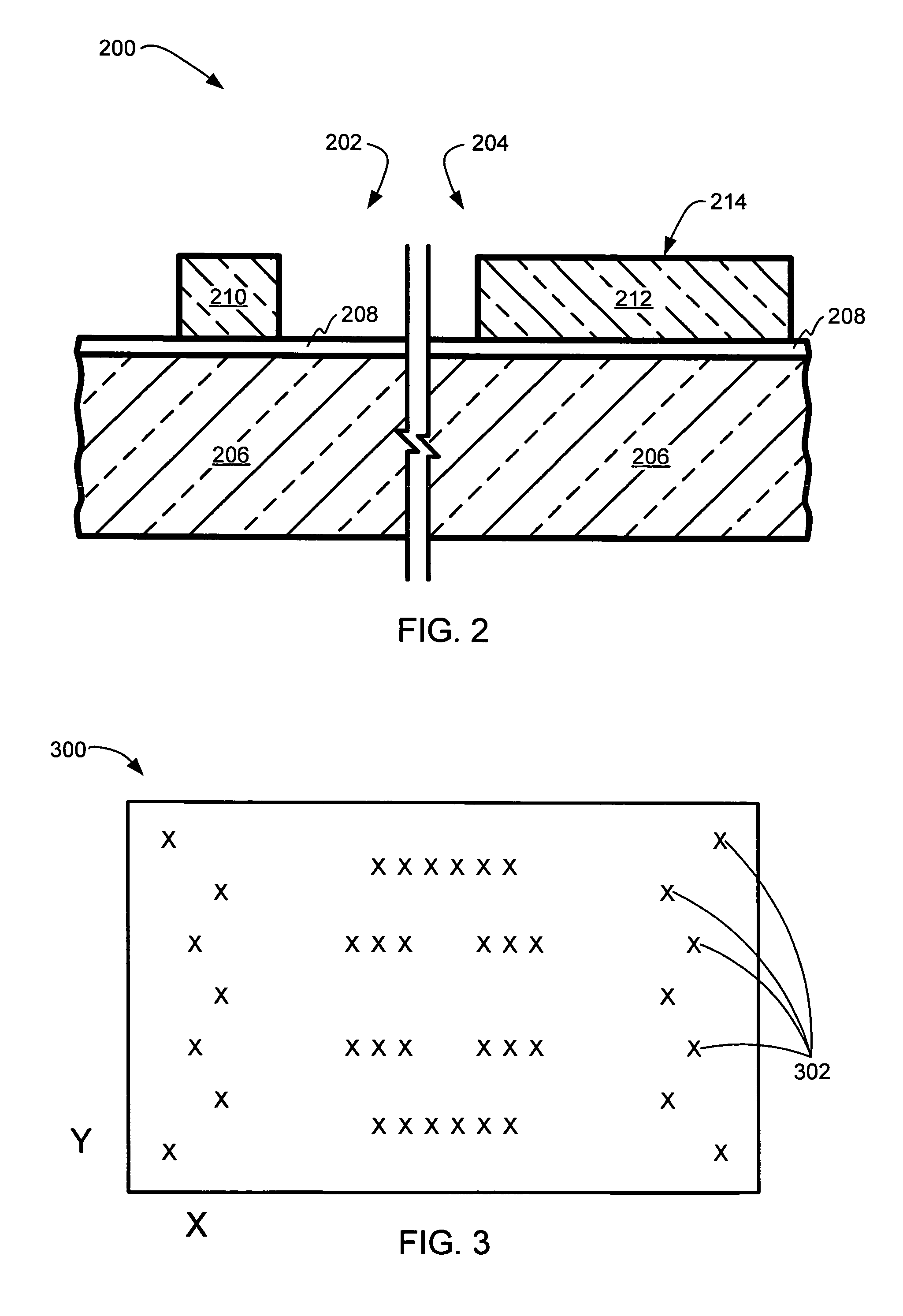
A method for determination of tunnel oxide weakness is provided. A tunnel oxide layer is formed on a semiconductor wafer. At least one poly gate is formed on the tunnel oxide layer in a flash memory region of the semiconductor wafer. At least one poly island, which is substantially larger than the poly gate, is formed on the tunnel oxide layer in a voltage contrast cell region of the semiconductor wafer. The poly island and the tunnel oxide layer therebeneath form a voltage contrast tunnel oxide cell. A voltage contrast measurement is performed on the voltage contrast tunnel oxide cell. The voltage contrast measurement is then compared with prior such voltage contrast measurements on other such voltage contrast tunnel oxide cells. The tunnel oxide weakness of the tunnel oxide layer is then determined from the voltage contrast measurement comparisons.

Description

BACKGROUND[0001]1. Technical Field[0002]The present invention relates generally to semiconductor technology, and more specifically to semiconductor research and development.[0003]2. Background Art[0004]At the present time, electronic products are used in almost every aspect of life, and the heart of these electronic products is the integrated circuit. Integrated circuits are used in a wide variety of products, such as televisions, telephones, and appliances.[0005]Integrated circuits are made in and on silicon wafers by extremely complex systems that require the coordination of hundreds or even thousands of precisely controlled processes to produce a finished semiconductor wafer. Each finished semiconductor wafer has hundreds to tens of thousands of integrated circuits, each worth hundreds or thousands of dollars.[0006]The ideal would be to have every one of the integrated circuits on a wafer functional and within specifications, but because of the sheer numbers of processes and minu...

Claims


Application Information

Patent Timeline
IPC IPC(8): H01L21/00
CPCG01R31/307G11C29/006G11C29/50G11C29/56008G11C29/56G01R31/2831G11C16/04G11C2029/5602G11C2029/0403G11C2029/4002G11C2029/5004
Inventor WANG, JOHN J.ERHARDT, JEFFREY P.HILL, WILEY EUGENE
Owner ADVANCED MICRO DEVICES INC
Why Eureka
Try Eureka