Advanced seed layery for metallic interconnects

a technology of metallic interconnects and seed layers, which is applied in the direction of semiconductor devices, semiconductor/solid-state device details, electrical apparatus, etc., can solve the problems of poor or incomplete filling (voids) of high ar openings, the cvd of ald techniques is generally much slower than the other cvd techniques, and the openings are often small in size and shape, etc., to achieve high aspect ratios

Inactive Publication Date: 2006-09-12
COHEN URI DR
View PDF72 Cites 23 Cited by
  • Summary
  • Abstract
  • Description
  • Claims
  • Application Information

AI Technical Summary

Problems solved by technology

However, the ALD techniques are generally much slower than the other CVD techniques.
Further, the higher the AR of the openings, the slower the electroplating rate is inside.
This results in poor or incomplete filling (voids) of high AR openings, when compared with results achieved with low AR openings.
Further, growth inhibition inside the openings is decreased from that achieved outside the openings due to slow replenishment of the additives inside the openings as compared with replenishment of the additives on the field.
Any voltage drop (and resulting non-uniformity therefrom) becomes more severe with increasing wafer size (200 mm to 300 mm), and as the resistance of the seed layer increases due to insufficient thickness and / or high resistivity.
However, the typical conformal seed layer thickness of about 300 Å to about 800 Å (on the field), deposited by the CVD or electroless techniques, may not be sufficient.
Neither of these techniques satisfies all of the above-identified requirements.
The non-conformal PVD techniques, while providing adequate thickness on the field, fail to provide continuous and complete sidewall and / or bottom coverage inside very narrow openings with large AR.
They also result in substantial overhangs at the top corners of the openings.
As a result, typical conformal seed layers are too thin on the field and too thick inside the very narrow openings.

Method used


Image

  • Advanced seed layery for metallic interconnects
  • Advanced seed layery for metallic interconnects
  • Advanced seed layery for metallic interconnects

Examples


example 1

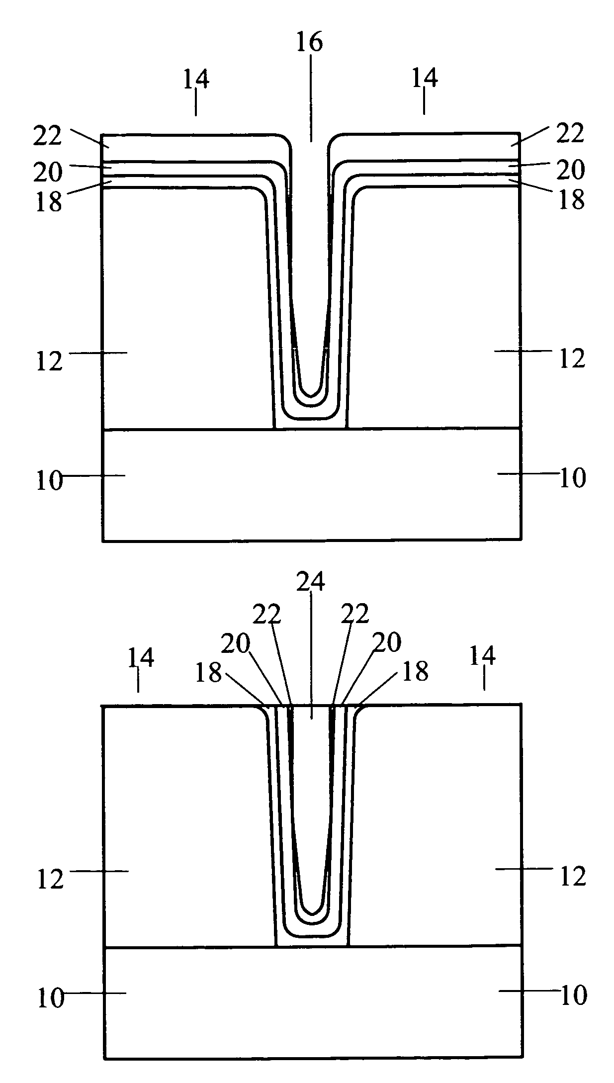
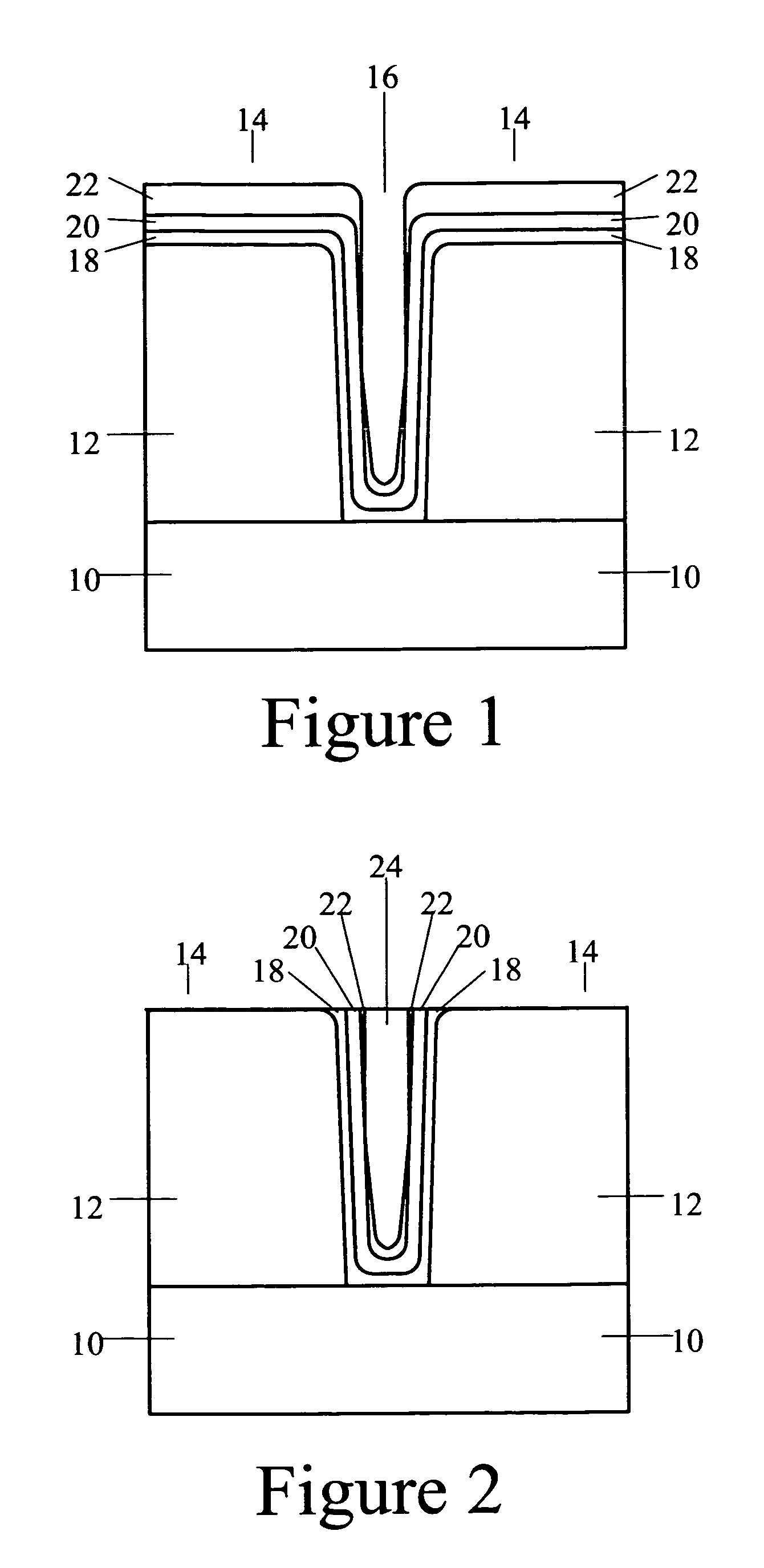
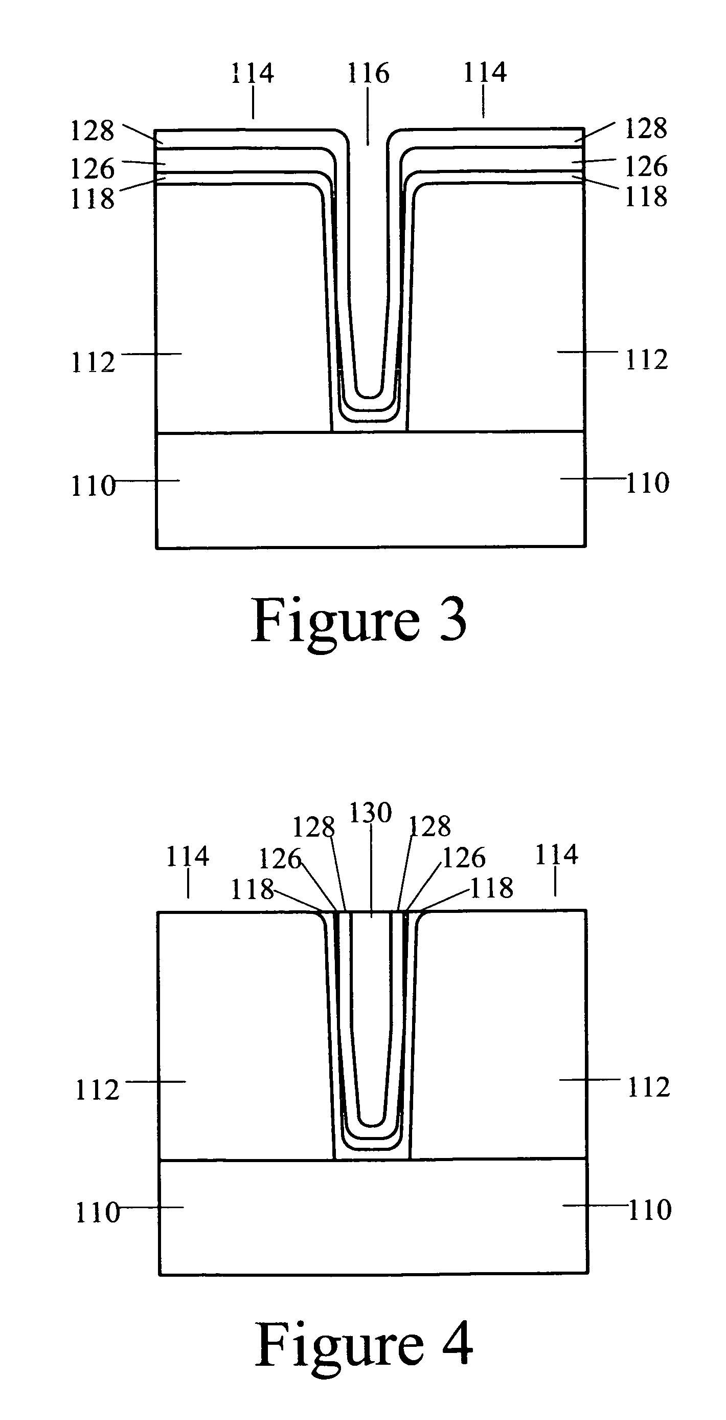
[0031]The following presents an example of an embodiment of the inventive method for 0.18 μm wide vias or trenches. In accordance with this embodiment, one deposits, by a CVD technique, a barrier layer comprised of about 200 Å of TaNX or WNX, then one deposits, by a CVD technique, a conformal seed layer comprised of about 300 Å of Cu, finally one deposits, by a PVD technique, a non-conformal seed layer comprised of about 900 Å of Cu (as measured on the field). This will result in a total combined (including the barrier) thickness of about 400 Å inside the openings: {Cu(PVD˜50 Å) / Cu(CVD˜250 Å) / TaNx(CVD˜100 Å)} and a total combined Cu seed layers and barrier layer thickness of about 1,400 Å on the field: {Cu(PVD˜900 Å) / Cu(CVD˜300 Å) / TaNx(CVD˜200 Å}. Advantageously, in accordance with the present invention, the inventive “two-step” seed layer deposition ensures a continuous seed layer having excellent step coverage, and a low-resistance electrical path on the field to ensure uniform co...

example 2

[0048]FIGS. 5 and 6 show scanning electron microscope (“SEM”) photographs of a cross-section of a 0.10 μm wide trench having Cu seed layers prepared in accordance with one embodiment of the invention. In accordance with this embodiment, a pattern of trenches was formed in a SiO2 insulating layer. The trenches were about 0.10 μm wide (at their bottom) and about 1.4 μm deep (thereby having an aspect ratio of about 14:1). Next, a barrier layer (WNX) was deposited using a CVD technique. Next, a relatively thin, conformal Cu seed layer was deposited using a CVD technique. The barrier layer and thin, conformal Cu seed layer is seen at 501 in FIG. 6. In accordance with this embodiment, the combined thickness of the barrier and the CVD Cu seed layer was about 500 Å on the field, and about 400–500 Å on the sidewalls and bottom of the trenches. Next, a non-conformal PVD Cu seed layer having a thickness of about 1,400 Å (on the field) was deposited by sputtering. In this embodiment, the non co...

example 3

[0049]Similar to Example 2 above, trenches ˜0.10 μm wide (at their bottom) and ˜1.4 μm deep (thereby having an aspect ratio of ˜14:1) were formed in a SiO2 insulating layer. Next, a barrier layer (WNX) was deposited using a CVD technique. Next, a relatively thin, conformal Cu seed layer was deposited using a CVD technique. The combined thickness of the barrier layer and the CVD Cu layer was ˜500 Å on the field, and ˜400–500 Å on the sidewalls and bottom of the trenches. Next, a non-conformal PVD Cu seed layer having a thickness of ˜500 Å (on the field) was deposited by sputtering. The end result was a combined thickness (including the barrier layer and the Cu seed layers) of only about 400–500 Å on the sidewalls and bottom of the trenches (with excellent continuity and uniformity there), and about 1,000 Å on the field, without pinching-off the trenches.

[0050]It should be understood that the scope of the present invention is not limited to the embodiments described above with respect...


PUM


Abstract

One embodiment of the present invention is a method for making metallic interconnects, which method is utilized at a stage of processing a substrate having a patterned insulating layer which includes at least one opening and a field surrounding the at least one opening, the field and the at least one opening being ready for depositing one or more seed layers, which method includes steps of: (a) depositing by an ALD technique at least an initial portion of a substantially conformal seed layer on the field and inside surfaces of the at least one opening, wherein said at least one opening has a width of less than about 0.13 μm; (b) depositing by a PVD technique a substantially non-conformal seed layer over the substantially conformal seed layer, said substantially non-conformal seed layer being thicker than said substantially conformal seed layer over the field; and (c) electroplating a metallic layer over the substantially non-conformal seed layer, wherein the electroplated metallic layer consists of a material selected from a group consisting of Cu, Ag, or alloys comprising one or more of these metals.

Description

[0001]This is a continuation of a patent application entitled “Methods for Making Multiple Seed Layers for Metallic Interconnects”, Ser. No. 10 / 328,629, filed on Dec. 23, 2002 now U.S. Pat. No. 6,924,226, which itself is a continuation-in-part of a patent application entitled “Multiple Seed Layers for Metallic Interconnects”, Ser. No. 09 / 730,220, filed on Dec. 4, 2000, now U.S. Pat. No. 6,518,668, which itself is a continuation-in-part of a patent application entitled “Seed Layers for Interconnects and Methods and Apparatus for Their Fabrication”, Ser. No. 09 / 563,733, filed on May 3, 2000, now U.S. Pat. No. 6,610,151, which itself is a continuation-in-part of a patent application entitled “Seed Layers for Interconnects and Methods for Fabricating Such Seed Layers”, Ser. No. 09 / 410,898, filed on Oct. 2, 1999, now U.S. Pat. No. 6,136,707 which issued on Oct. 24, 2000.TECHNICAL FIELD OF THE INVENTION[0002]The present invention pertains to the field of electroplating metals or alloys on...

Claims


Application Information

Patent Timeline
Patent Type & Authority Patents(United States)
IPC IPC(8): H01L21/4763H01L21/768
CPCH01L21/2855H01L21/28556H01L21/76843H01L23/53252H01L23/53238H01L21/76873H01L2221/1089H01L2924/0002H01L2924/00H01L23/528H01L23/53209
Inventor COHEN, URI
Owner COHEN URI DR
Why Eureka
Try Eureka