High voltage integrated circuit driver with a high voltage PMOS bootstrap diode emulator

a diode emulator and integrated circuit technology, applied in logic circuit coupling/interface arrangement, pulse automatic control, pulse technique, etc., can solve the problems of circuit reducing the complexity of the body diode circuitry, increasing fabrication cost and circuit complexity, and increasing process complexity and expens

Active Publication Date: 2006-09-12
SEMICON COMPONENTS IND LLC
View PDF4 Cites 23 Cited by
  • Summary
  • Abstract
  • Description
  • Claims
  • Application Information

AI Technical Summary

Problems solved by technology

External discrete components increase fabrication cost and the complexity of the circuit.
This circuit reduces the complexity of the body diode circuitry, however, it considerably increases the process complexity and expense with the introduction a high voltage JFET structure.

Method used


Image

  • High voltage integrated circuit driver with a high voltage PMOS bootstrap diode emulator
  • High voltage integrated circuit driver with a high voltage PMOS bootstrap diode emulator
  • High voltage integrated circuit driver with a high voltage PMOS bootstrap diode emulator

Examples


Embodiment Construction

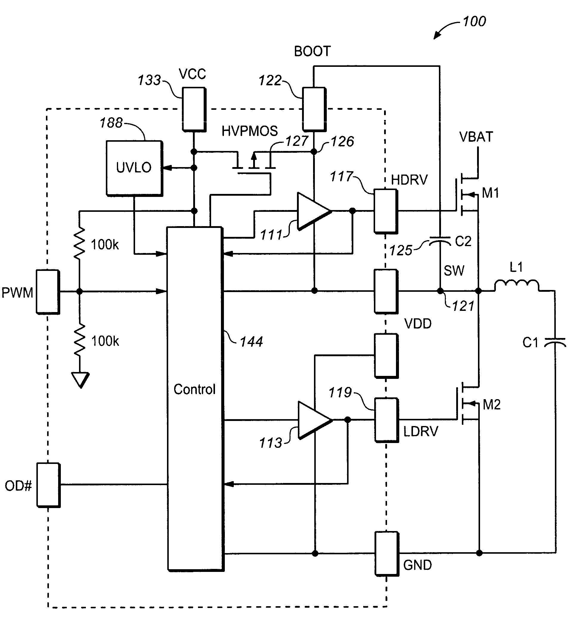
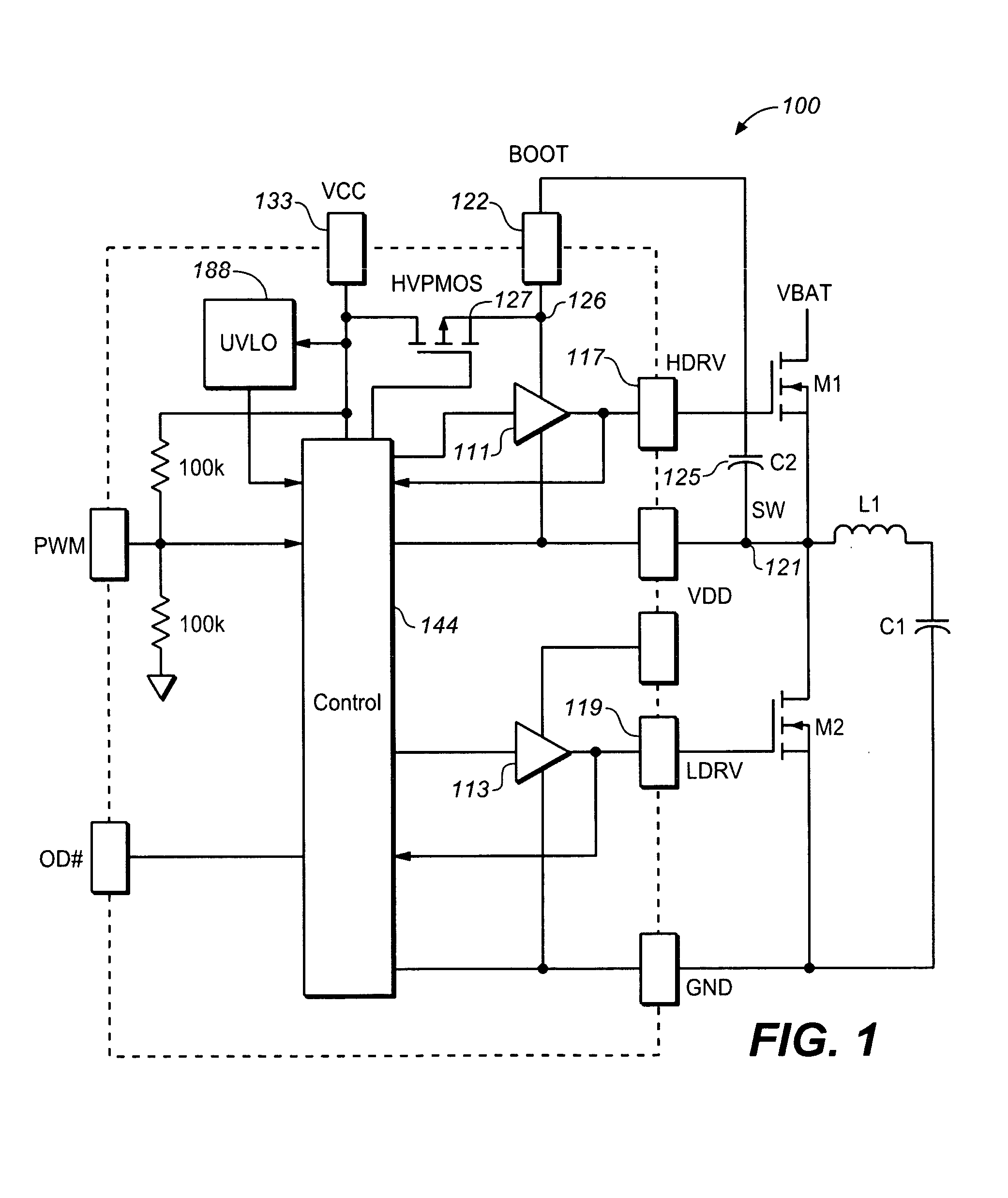
[0018]Embodiments of the present invention are best understood by referring to FIGS. 1–4 of the drawings. Like numerals are used for like and corresponding parts of the various drawings.

[0019]FIG. 1 illustrates a high voltage circuit driver100 according to an embodiment of the invention. Circuit driver 100 includes a high side driver cell 111, which can be coupled to a gate of a high side power MOSFET M1, and a low side driver cell 113, which can be coupled to a gate of a low side power MOSFET M2. Power MOSFETs M1 and M2 can be N-channel MOSFETs. In some embodiments, circuit driver 100 is separate from power MOSFETs M1 and M2. In these embodiments, high side driver cell 111 is coupled to high side power MOSFET M1 via high side drive port 117, and low side driver cell 113 is coupled to low side power MOSFET M2 via low side drive port 119. In other embodiments circuit driver 100 and power MOSFETs M1 and M2 are integrated.

[0020]High side power MOSFET M1 is coupled between a power suppl...


PUM


Abstract

A high voltage circuit driver includes high and low side driver cells to drive a high and a low side power MOSFET, a bootstrap circuit to energize the high side driver cell, a high voltage PMOS transistor (HVPMOS) between a voltage source and the bootstrap circuit, wherein the HVPMOS is embedded in an N-isolation layer and is integrated with the driver cells. A bootstrap control circuit, for controlling the HVPMOS, includes a high voltage level shift stage, which can also be embedded in an N-isolation layer. The circuit driver is operated by switching the high side drive signal from high to low, the low side drive signal from low to high with a first delay, and a bootstrap control signal from high to low with an additional second delay. Also, the bootstrap capacitor is first charged by switching on the HVPMOS, and then it energizes the high side driver cell.

Description

BACKGROUND[0001]1. Field of Invention[0002]The present invention relates to drivers for DC-to-DC converters and more particularly to high voltage drivers with diode emulators.[0003]2. Description of Related Art[0004]Various DC-to-DC converters and related circuits often use two power MOSFETs, which are connected at an output node in a half-bridge configuration. The output node is connected to an inductor-capacitor filter. Such DC-to-DC converters allow the conversion of variable input battery voltages in a wide range, for example in the range of 6–24V to be stepped down to a lower constant output voltage. When the battery voltage decays from a nominal value of 24V to a value as low as 6V, the output voltage of the DC-to-DC converter remains essentially constant, because of the adaptive adjustments of the converter.[0005]A converter includes a driver circuit, which drives the power MOSFETs. The driver circuit is controlled by a control circuit to turn on the high side power MOSFET an...

Claims


Application Information

Patent Timeline
Patent Type & Authority Patents(United States)
IPC IPC(8): H03K19/094H03K19/0175H03K19/082H03L7/06
CPCH03F3/2171H03K19/01735H03K17/063H03K17/6871H03F2200/31H03F2200/351H02M1/08H02M3/155
Inventor BRYSON, STEPHEN W.
Owner SEMICON COMPONENTS IND LLC
Why Eureka
Try Eureka