Multi-site chip carrier and method

a chip carrier and multi-site technology, applied in the direction of coupling device connection, coupling parts engagement/disengagement, instruments, etc., can solve the problem of limited number of ic packages tested on a single board, and achieve the effect of reducing the number of socket devices, reducing the number of times a test operator has to open and close the socket, and increasing the number of ic packages tested

Inactive Publication Date: 2006-09-19
WELLS CTI LLC
View PDF6 Cites 20 Cited by
  • Summary
  • Abstract
  • Description
  • Claims
  • Application Information

AI Technical Summary

Benefits of technology

[0004]It is therefore desirable both to increase the number of IC packages tested on a single board and correspondingly reduce the number of socket devices, thereby reducing the number of times a test operator has to open and close sockets. It would be advantageous to have a socket that accommodates multiple IC packages within a single socket. More IC packages could then be tested on a single board and less time would be spent per IC package opening and closing sockets, thereby decreasing the cost of IC package manufacturing. It would also be advantageous to have a socket that accommodates more than one type or size of IC package within a single socket.

Problems solved by technology

However, the number of IC packages tested on a single board is limited to the number of sockets that can fit on the printed circuit board.

Method used


Image

  • Multi-site chip carrier and method
  • Multi-site chip carrier and method
  • Multi-site chip carrier and method

Examples


Embodiment Construction

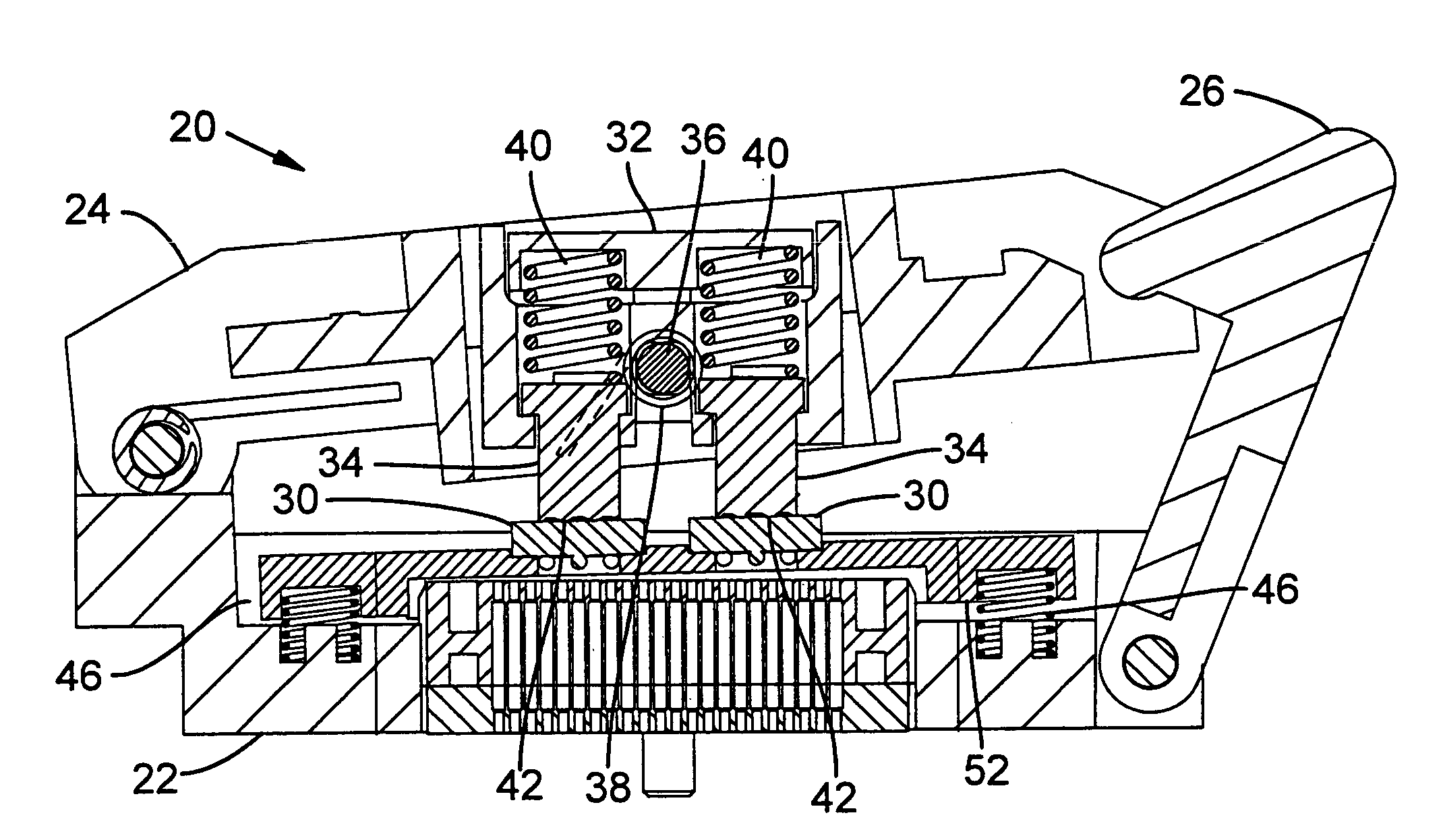
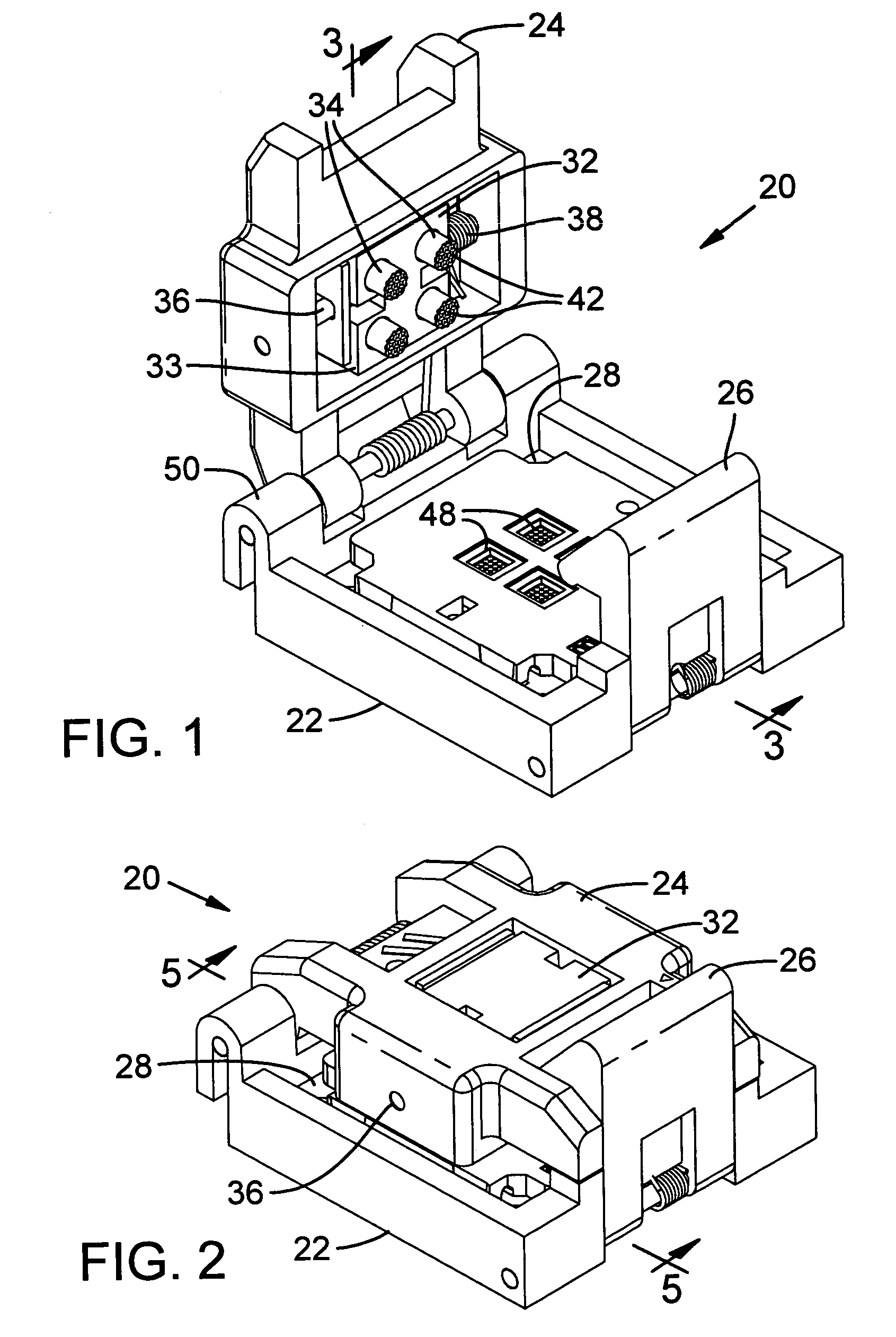
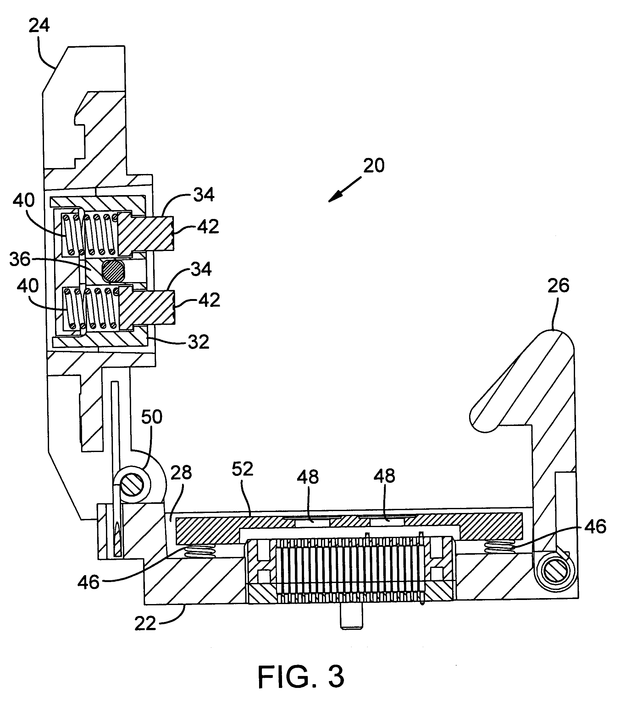
[0013]FIGS. 1 and 2 are perspective views of the preferred embodiment of the IC package socket device 20 according to the invention in opened and closed positions, respectively. The IC package socket device has a base 22 and a lid 24 that is latched closed onto the base 22 by a latch 26. IC package receiver area 28 in the base 22 receives multiple IC packages 30 (shown in FIGS. 4 and 5). The receiver area 28 is arranged with an array of recesses 48 to receive two or more (e.g., four) IC packages 30. The socket device can be arranged to receive a die or a packaged die and the term IC package hereinafter will encompass either option. The socket device can also be arranged to receive more than one type or size of IC package thereby increasing the versatility and usefulness of the socket device.

[0014]The lid 24 is attached to the base 22 through hinge 50. The latch 26 is positioned opposite hinge 50. A multi-site pressure unit 32 is positioned within the lid 24 in alignment, when closed...


PUM


Abstract

An integrated circuit (IC) package socket device that can receive two or more IC packages and the method of operating the device. Uses for the device include burn-in in which testing and programming of dies or completed IC packages. The device can also be arranged to receive two or more types of IC packages. A pressure unit is tiltably attached to the lid of the socket device providing a resilient normal force to each of the two or more IC packages without damaging the IC packages. The pressure unit has two or more pressure pads that correspondingly apply the resilient normal force to each of the two or more IC packages. The IC packages are received in recesses where the recesses are typically arranged in an array with the pressure pads in the pressure unit arranged so as to align with the array of recesses.

Description

FIELD OF THE INVENTION[0001]This invention relates to integrated circuit socket devices.BACKGROUND AND SUMMARY OF THE INVENTION[0002]Integrated circuit (IC) packages must be tested after their manufacture. Testing can include burn-in, testing and programming of IC packages. The integrated circuits are temporarily installed on a circuit board, tested, and then removed from the circuit board. Accordingly, sockets are necessary to install the IC packages on the printed circuit board for testing. These sockets include multiple contacts to connect each of the terminals of the IC package to corresponding conductors on the printed circuit board. Currently, each IC package is tested in a separate socket requiring a test operator to open and close each socket each time an IC is tested. An example of such a socket is the Wells-CTI socket series number 654.[0003]The sockets are positioned on a printed circuit board where the sockets are arranged in a relatively dense array to allow for as many...

Claims


Application Information

Patent Timeline
Patent Type & Authority Patents(United States)
IPC IPC(8): H01R12/00
CPCG01R1/0466
Inventor HARPER, PATRICK HENRY
Owner WELLS CTI LLC
Why Eureka
Try Eureka