Differential gain stage for low voltage supply

a gain stage and low voltage technology, applied in the direction of amplifiers, amplifiers with semiconductor devices/discharge tubes, electrical equipment, etc., can solve the problems of limiting the common mode operating range of differential pair transistors, and causing several problems

Inactive Publication Date: 2006-09-19
DIALOG SEMICONDUCTOR GMBH
View PDF9 Cites 12 Cited by
  • Summary
  • Abstract
  • Description
  • Claims
  • Application Information

AI Technical Summary

Benefits of technology

[0010]A principal object of the present invention is to provide an effective and very manufacturable circuit device.
[0013]A yet further object of the present invention is to provide a differential stage circuit device with bulk forward biasing of the differential MOS transistor pair to improve low voltage performance.
[0017]In accordance with the objects of this invention, a method to improve the low voltage performance of a differential gain stage is achieved. The method comprises providing a monitoring stage and a differential stage. The monitoring stage comprises a differential transistor pair having a first differential input, a second differential input, an upper current input, and a lower current output. In addition, a current source is connected to the upper current input, and a current load is connected to the lower current output. The differential stage comprises a differential transistor pair having a first differential input, a second differential input, an upper current input, a first lower current output, and a second lower current output. In addition, a current source is connected to the upper current input, a first current load is connected to the first lower current input, and a second current load is connected to the second lower current input. A current is forced through the monitoring stage current source. The current through the monitoring stage current source is mirrored in the differential stage current source. Current through the monitoring stage current load is mirrored through the differential transistor stage first and second current loads. The monitoring stage and the differential stage first differential inputs are forced to the same voltage. The monitoring stage and the differential stage second differential inputs are forced to the same voltage.

Problems solved by technology

If the supply voltage drops to a very low level of, for example, about 1 V and, further, if the threshold voltage of the MOS transistors is about 0.65 V, then several problems may occur.
Second, the small voltage difference between the power supply and the threshold voltage of the MOS transistors will limit the common mode operating range of the differential pair transistors 26 and 28.

Method used


Image

  • Differential gain stage for low voltage supply
  • Differential gain stage for low voltage supply
  • Differential gain stage for low voltage supply

Examples


first embodiment

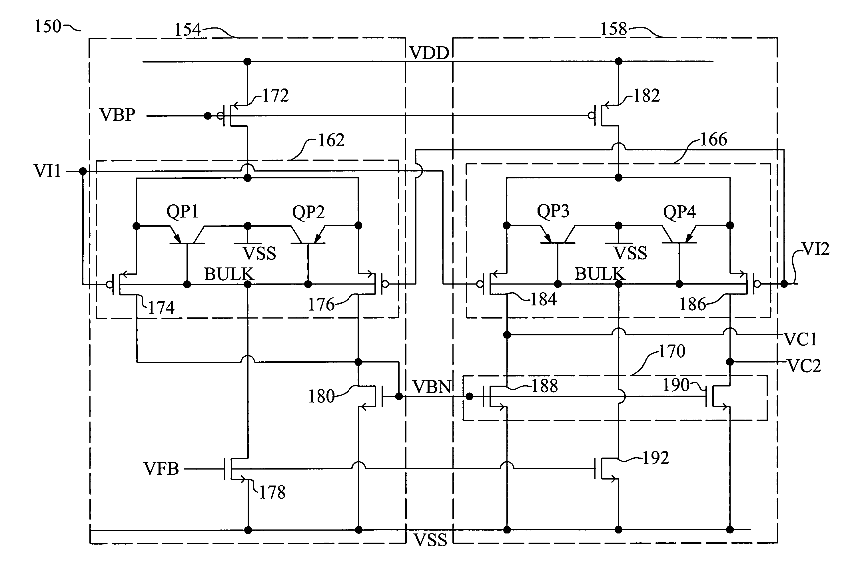
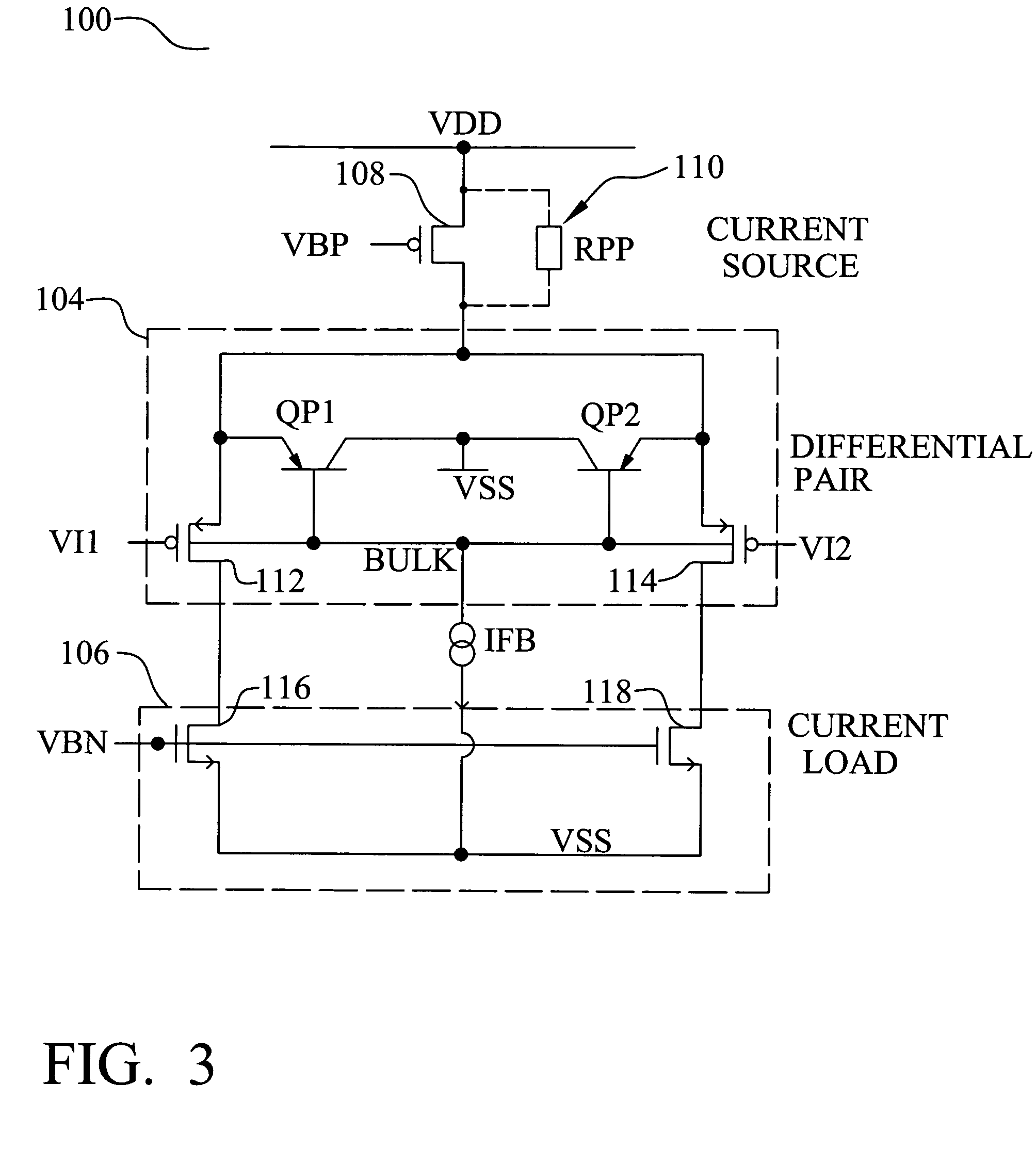
[0033]Referring now to FIG. 4, a second preferred embodiment of the present invention is illustrated. In this embodiment, a means for compensating the variation in current source performance and parasitic substrate current is achieved. This differential stage circuit 150 comprises a monitoring stage 154 and a differential pair stage 158. The differential pair stage 158 is essentially the same as that shown in the first embodiment in FIG. 3. In particular, a differential pair 166 comprises common source connected first and second transistors 184 and 186. The gates of the first and second transistors 184 and 186 are connected to the first and second differential inputs VI1 and VI2, respectively. A current source transistor 182 is connected to the current source input of the differential pair 166. A current load 170 comprising first and second transistors 188 and 190 is connected to the drains of the differential pair transistors 184 and 186 to form the output voltage signals VC1 and V...

embodiment 200

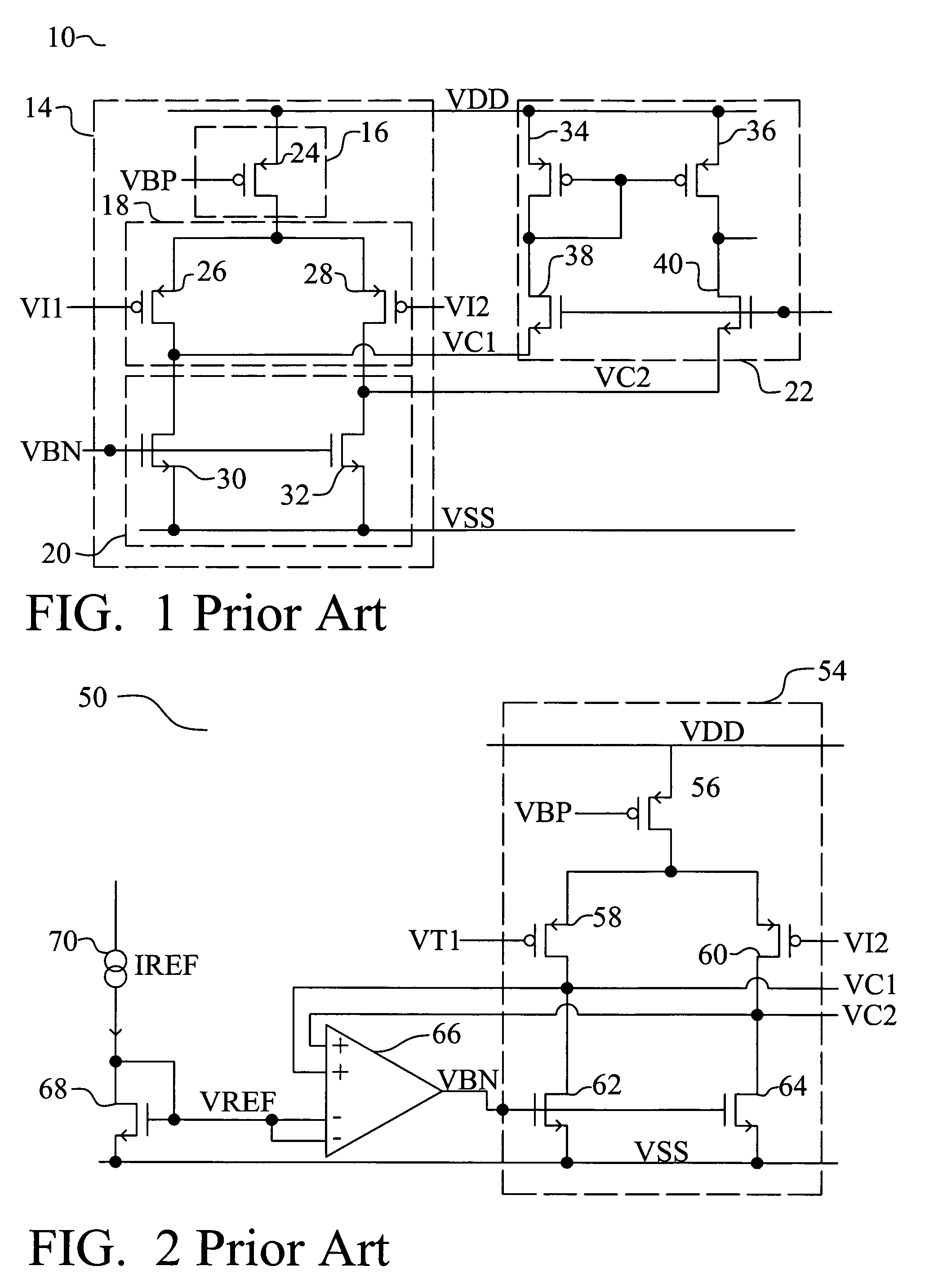
[0037]Referring now to FIG. 5, a third preferred embodiment 200 of the present invention illustrated. In this case the differential pair stage 204 is used in a comparator or for low voltage startup of a bandgap reference. The differential pair stage 204 and the monitoring stage 208 are constructed as described before. In this case, the first bias voltage VBP, used to control the current source, and the forward bias voltage VFB, used to control before bias current source, are generated from a current reference IREF. The second bias voltage VBN is again generated by the monitoring stage 208 and provides a means to compensate the differential pair stage 204 over voltage and parasitic current conditions. The output VC2 of the differential pair stage 204 provides the startup control for the bandgap section to generate the bandgap bias voltage VBIAS.

[0038]Referring now to FIG. 6, a fourth preferred embodiment of the present invention is shown. In this variation of the circuit, the input c...


PUM


Abstract

A new method and a circuit to improve the low voltage performance of a differential gain stage is achieved. The method comprises a monitoring stage and a differential stage. The monitoring stage comprises a differential transistor pair having first and second differential inputs, an upper current input, and a lower current output. In addition, a current source is connected to the upper current input, and a current load is connected to the lower current output. The differential stage comprises a differential transistor pair having first and second differential inputs, an upper current input, and first and second lower current outputs. In addition, a current source is connected to the upper current input, and first and second current loads are connected to the first and second lower current inputs. A current is forced through the monitoring stage current source. The current through the monitoring stage current source is mirrored in the differential stage current source. Current through the monitoring stage current load is mirrored through the differential transistor stage first and second current loads.

Description

BACKGROUND OF THE INVENTION[0001](1) Field of the Invention[0002]The invention relates to an integrated circuit device, and, more particularly, to a differential gain stage capable of low voltage operation.[0003](2) Description of the Prior Art[0004]Differential gain stages are used in a large variety of electronics circuits. Differential gain stages provide a means of buffering signals and of multiplying voltage and / or current differences between signals. Differential gain stages are one of the key functional features in operational amplifier and / or comparator designs. Differential gain stages typically comprise a pair of transistors. These transistors may be bipolar or MOS.[0005]Referring now to FIG. 1, an example of a prior art differential stage circuit 10 is shown. This differential stage circuit comprises a differential stage 14 and a folded cascode structure 22. The differential stage 14 further comprises a differential pair made up of a first MOS transistor 26 and a second M...

Claims


Application Information

Patent Timeline
Patent Type & Authority Patents(United States)
IPC IPC(8): H03F3/45
CPCH03F3/45183H03F3/45282H03F3/45291H03F2203/45521H03F2200/78H03F2203/45398H03F2200/513
Inventor KILLAT, DIRK
Owner DIALOG SEMICONDUCTOR GMBH
Why Eureka
Try Eureka