Integrated optical device including a vertical lasing semiconductor optical amplifier

a semiconductor optical amplifier and integrated optical device technology, applied in semiconductor lasers, laser details, electrical devices, etc., can solve the problems of optical signal attenuation, signal distortion, crosstalk, etc., to accelerate the adoption and development of optical technologies

Inactive Publication Date: 2006-09-19
II VI DELAWARE INC
View PDF14 Cites 13 Cited by
  • Summary
  • Abstract
  • Description
  • Claims
  • Application Information

AI Technical Summary

Benefits of technology

[0023]The present invention is particularly advantageous because the integration of VLSOAs with other optical elements on a common substrat

Problems solved by technology

In these systems, phenomena such as fiber losses, losses due to insertion of components in the transmission path, and splitting of the optical signal may attenuate the optical signal and degrade the corresponding signal-to-noise ratio as the optical signal propagates through the communications system.
Thus, strong portions of the optical signal are amplified less than weak portions, resulting in distortion of the signal and also crosstalk between different optical signals propagating simultaneously through the amplifier.
This significantly limits the use of conventional SOAs.
Current-day optical amplifiers, however, are not suited to play an analogous role with respect to integrated optics.
For example, fiber amplifiers are inherently too large to be useful in integrated optics.
Fiber amplifiers also suffer from slow switching speeds and poor power efficiency.
As a result, not only is it difficult to produce large quantities of fiber amplifiers but the fiber amplifiers produ

Method used


Image

  • Integrated optical device including a vertical lasing semiconductor optical amplifier
  • Integrated optical device including a vertical lasing semiconductor optical amplifier
  • Integrated optical device including a vertical lasing semiconductor optical amplifier

Examples


Embodiment Construction

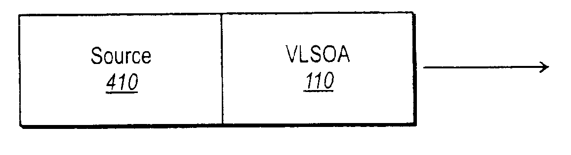
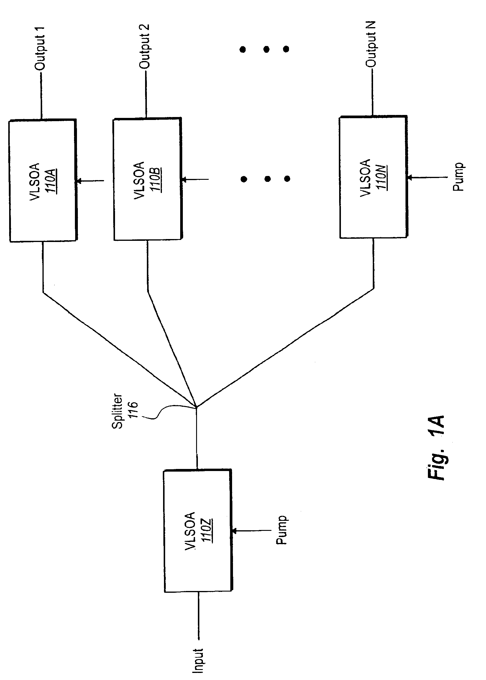
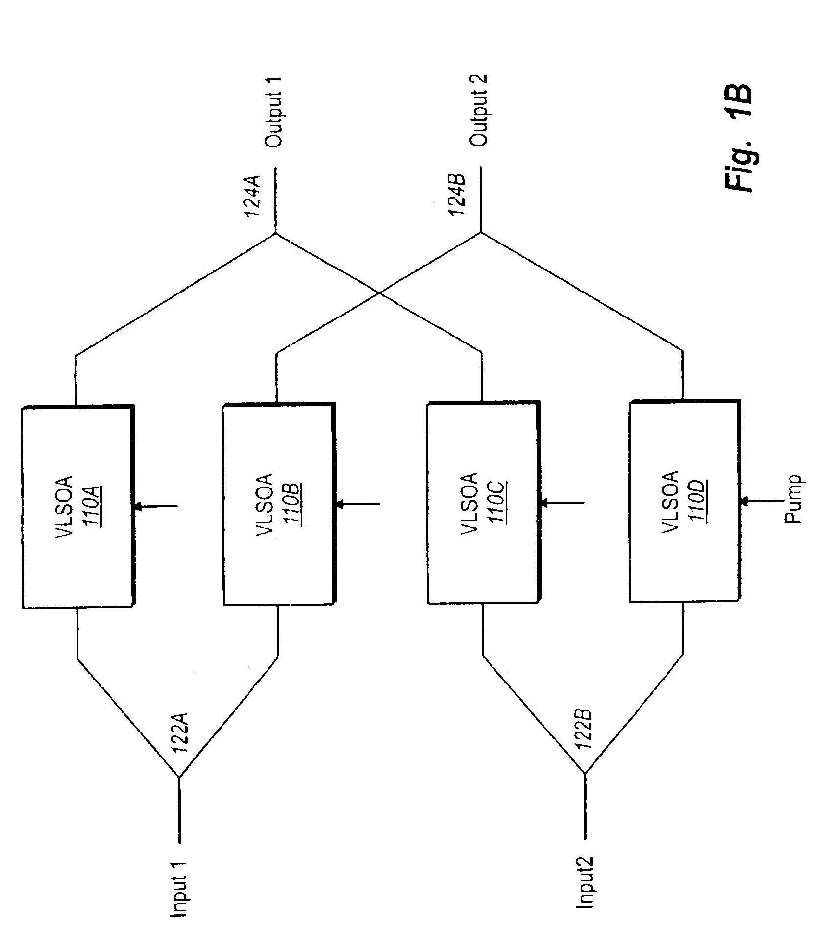
[0037]FIGS. 1A-4E are block diagrams of example integrated optical devices according to the present invention. Each example device includes a vertical lasing semiconductor optical amplifier (VLSOA) 110 and at least one other optical element integrated onto a common substrate. In some embodiments, the VLSOA and other optical element are optically coupled together on the integrated optical device, either directly or indirectly. For example, an output of the VLSOA may be coupled to an input of the optical element, the output of the optical element may be coupled to an input of the VLSOA, and / or the VLSOA and optical element may both be coupled to a common third optical element. In other embodiments, the VLSOA and other optical elements are integrated on a common substrate but they are not optically coupled to each other. For example, the integrated optical device might be a linear array of VLSOAs, with the inputs and outputs of the VLSOAs serving as inputs and outputs to the integrated...


PUM


Abstract

An intergrated optical device comprises a vertically lasing semiconductor optical amplifier (VLSOA) and an optical element integrated onto a common substrate. Example optical elements include waveguides, unguided transparent regions, and active optical devices (including additional VLSOAs). The integrated device may be fabricated using a number of different methods, including based on selective area epitaxy, impurity induced disordering, etch and fill and silicon optical bench.

Description

CROSS-REFERENCE TO RELATED APPLICATION[0001]This application claims priority under 35 U.S.C. § 119(e) to U.S. Provisional Pat. application Ser. No. 60 / 255,753, “Optical Devices Including a Semiconductor Optical Amplifier,” by Jeffrey D. Walker, et al., filed Dec. 14, 2000. The subject matter of all of the foregoing are incorporated herein by reference.BACKGROUND OF THE INVENTION[0002]1. Field of the Invention[0003]This invention relates generally to semiconductor optical amplifiers. More particularly, it relates to vertically lasing semiconductor optical amplifiers (VLSOAs) integrated with other optical elements on a common substrate and to methods for fabricating such integrated optical devices.[0004]2. Description of the Related Art[0005]Optical amplifiers, which boost the power of optical signals, are a basic building block for many types of optical systems. For example, fiber optic communications systems transmit information optically at very high speeds over optical fibers. A t...

Claims


Application Information

Patent Timeline
IPC IPC(8): H01S3/00
CPCH01S5/026H01S5/5027H01S5/1032H01S5/18311H01S5/5072H01S5/2027H01S5/2009
Inventor WALKER, JEFFREY D.DIJAILI, SOL P.
Owner II VI DELAWARE INC
Why Eureka
Try Eureka