
Sub-micron space liner and densification process

a space liner and sub-micron technology, applied in the direction of semiconductor/solid-state device manufacturing, basic electric elements, electric apparatus, etc., can solve the problems of increasing scaling difficulty for integrated circuit manufacturers, increasing the difficulty of filling these trenches with oxide, and pinching at the upper corners

Active Publication Date: 2006-09-26
MICRON TECH INC
View PDF13 Cites 86 Cited by
  • Summary
  • Abstract
  • Description
  • Claims
  • Application Information

AI Technical Summary

Benefits of technology

The patent describes methods for creating shallow trenches on a wafer and densifying liquid dielectric material. The methods involve depositing a liner on the trench surfaces, filling the trench with dielectric material, and expanding the liner to ensure a smooth transition. The invention also includes curing the substrate in a steam ambient environment and annealing it at a specific temperature to improve the quality of the final product. Additionally, the patent describes using an amorphous silicon layer to line the trench and fill it with a dielectric filler before expanding the liner and contracting the filler to achieve a smooth transition. Overall, the methods described in the patent improve the efficiency and reliability of the manufacturing process for semiconductor devices.

Problems solved by technology

Integrated circuit manufacturers increasingly face difficulties with scaling.
However, filling these trenches with oxide gets more challenging as the width of the trenches gets smaller and aspect ratios thus increase.
CVD deposits the material from the outside of the trench inwards, leading to pinching at the upper corners.
This leads to problems such as the creation of voids, areas where the filler does not accumulate, or to seams where the growth from the sides of the edges meets.
Such seams can create inconsistencies in subsequent processing, such as planarization or other etch steps.
HDP CVD methods can also result in undesired erosion of underlying features.
While spin-on can be more expensive and difficult to implement, it is seen as the long-range solution for the deposition of dielectric materials because of its ability to fill with no seam, void, or erosion problems.
However, there have been many problems with the implementation of trench-fill systems.
For the spin-on system, one of these problems has been achieving acceptable bulk density in sub-micron STI trenches.
However, available methods do not provide a full solution to the problems faced in this arena.
For example, the inventors have found that known methods of densification can lead to material that is too vulnerable to recess at the top of the trench during polishing and wet cleans.
Thus, the available solutions do not fully address the problems related to this area.

Method used


Image

  • Sub-micron space liner and densification process
  • Sub-micron space liner and densification process
  • Sub-micron space liner and densification process

Examples


Embodiment Construction

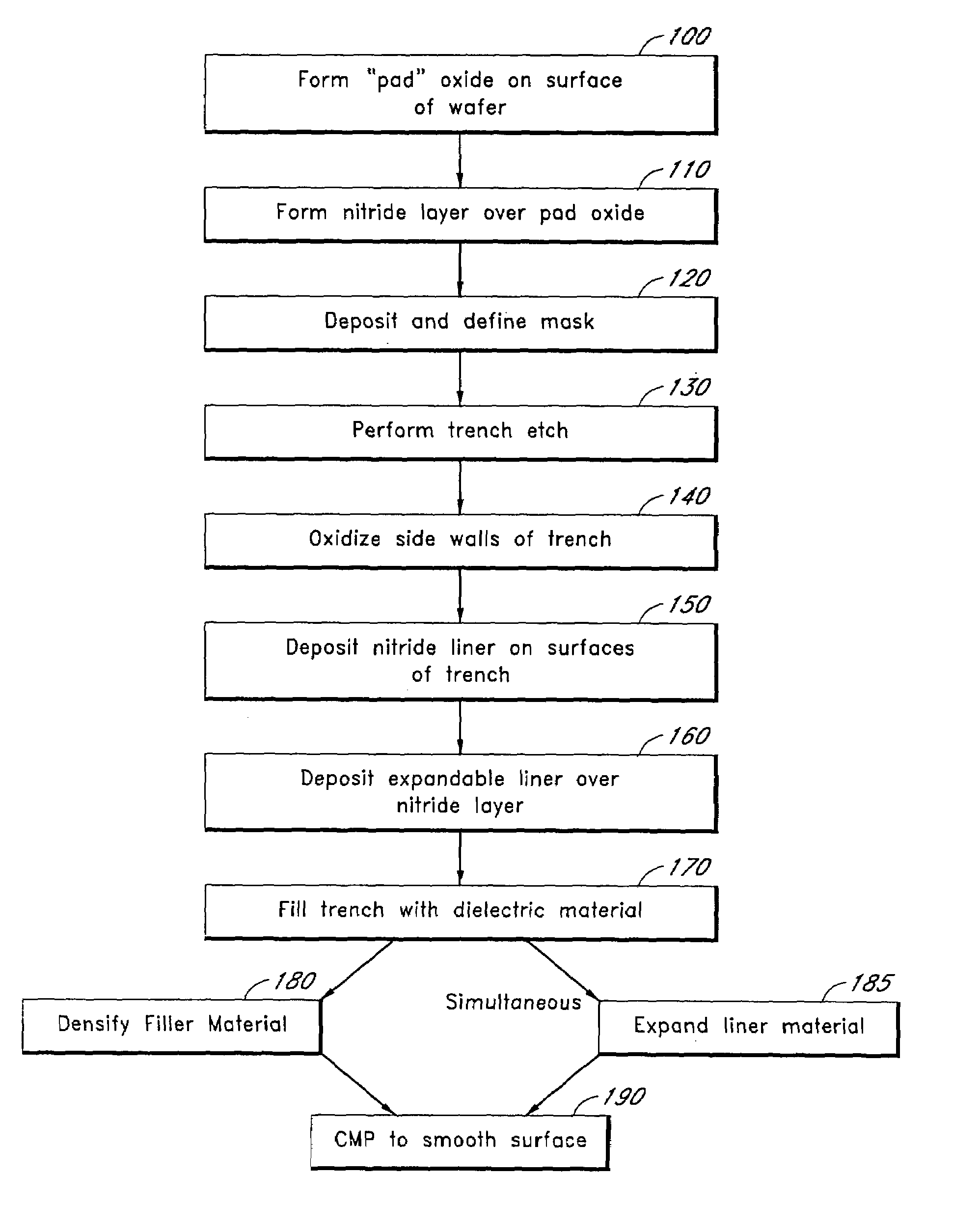
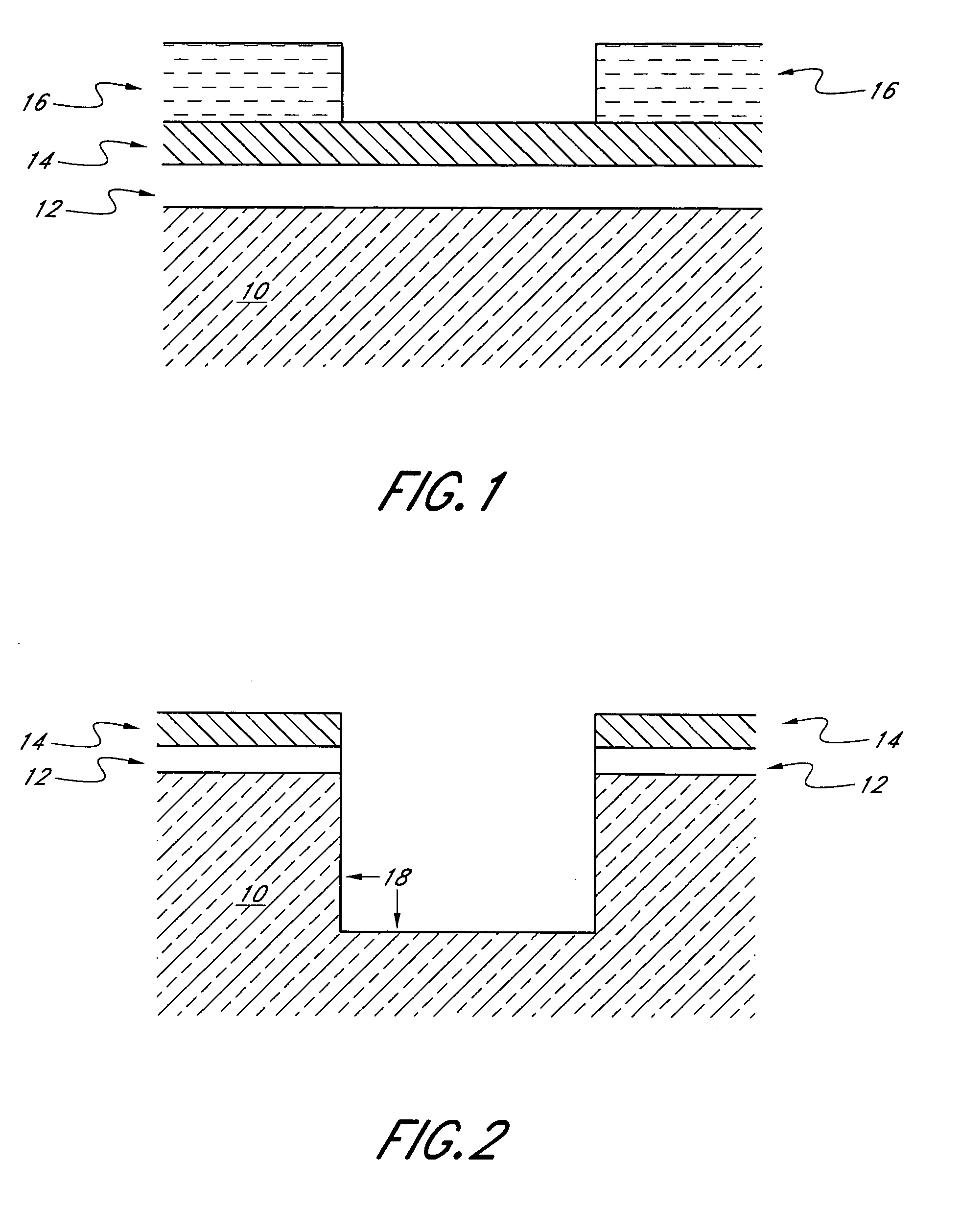
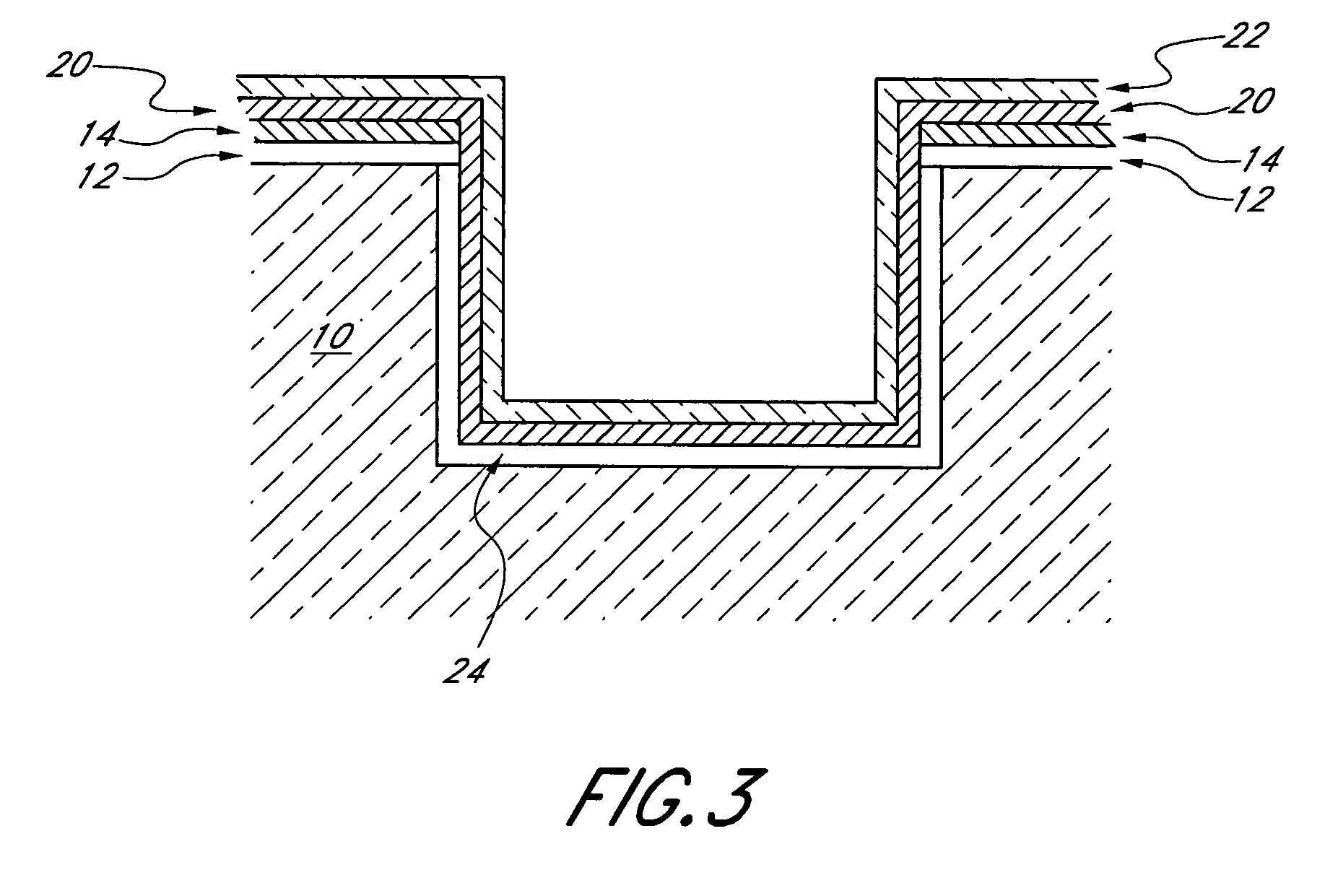
[0022]Bulk density of spin-on dielectric (SOD) materials can be achieved in sub-micron spaces, such as isolation trenches, through the use of a liner material that expands irreversibly when oxidized. In the illustrated embodiments described below, after a trench is formed, the sidewalls of the trench are oxidized, and a nitride layer is deposited to protect the active area of the trench. An expandable liner is deposited over the nitride liner before the trench is filled with a dielectric material. When the dielectric material is densified, the liner expands. The dielectric material reduces in size significantly as the material is densified. The expanding liner serves to evenly compress the dielectric material. In this manner, the combination of the liner and the densification process yields excellent bulk density in sub-micron spaces.

[0023]The liner material is preferably easily deposited in small spaces and irreversibly expanded when oxidized. In a preferred embodiment, the liner i...


PUM

PropertyMeasurementUnit
temperatureaaaaaaaaaa

Abstract

A method of depositing dielectric material into sub-micron spaces and resultant structures is provided. After a trench is etched in the surface of a wafer, an oxygen barrier is deposited into the trench. An expandable, oxidizable liner, preferably amorphous silicon, is then deposited. The trench is then filled with a spin-on dielectric (SOD) material. A densification process is then applied, whereby the SOD material contracts and the oxidizable liner expands. Preferably, the temperature is ramped up while oxidizing during at least part of the densification process. The resulting trench has a negligible vertical wet etch rate gradient and a negligible recess at the top of the trench.

Description

BACKGROUND OF THE INVENTION[0001]1. Field of the Invention[0002]This invention relates generally to the field of integrated circuit fabrication, and more specifically to the deposition and processing of spin-on dielectric materials.[0003]2. Description of the Related Art[0004]Integrated circuit manufacturers increasingly face difficulties with scaling. According to Moore's Law, the number of transistors per unit of area grows exponentially. For this to continue, several major changes in semiconductor manufacturing are expected. Transistors are not the only devices that must get smaller on an integrated circuit. Even though packing transistors closer is important, they must still be electrically separated from each other. One method of keeping transistors separate from each other is known as trench isolation. Trench isolation is the practice of creating trenches in the substrate in order to separate electrical components on the chip. The trenches are filled with an insulator that wil...

Claims


Application Information

Patent Timeline
Patent Type & Authority Patents(United States)
IPC IPC(8): H01L21/76H01L21/762
CPCH01L21/76224
Inventor SMYTHE, III, JOHN A.TRIVEDI, JIGISH D.
Owner MICRON TECH INC
Learn More