Module for optical device, and manufacturing method therefor

a technology of optical devices and modules, which is applied in the direction of radio frequency controlled devices, television systems, instruments, etc., can solve the problems of difficult to achieve a small-sized lens holder in terms of its structure, expensive adjustment systems and skilled workers, and insufficient time for the adjustment process

Active Publication Date: 2006-09-26
SHARP KK
View PDF13 Cites 32 Cited by
  • Summary
  • Abstract
  • Description
  • Claims
  • Application Information

AI Technical Summary

Benefits of technology

[0013]The invention is accomplished in view of the above-mentioned circumstances, and it is therefore an object of the invention to provide a small-sized and low cost module for an optical device that can be realized by that a focus adjuster for matching an optical distance between a lens and a solid-state image sensor with a focal length of the lens is not required. It is another object of the invention to provide a manufacturing method of a module for an optical device wherein a production process can be simplified since an adjusting process for matching an optical distance between a lens and a solid-state image sensor with a focal length of the lens is unnecessary.
[0031]Moreover, in the module for an optical device and its manufacturing method according to the invention, the bonding portion for bonding the solid-state image sensor and the transparent cover contains a photosensitive bonding agent, whereby the bonding portion is easily and efficiently formed with high precision by patterning with a photolithography technique. Further, the bonding portion can similarly be formed on either the solid-state image sensor and the transparent cover.

Problems solved by technology

In this adjusting process, an expensive system for the adjustment and a skilled worker are necessary and, further, a time required for the adjusting process is far from short.
Moreover, the lens holder has to have a function of two mechanism elements of the optical path demarcating unit and the focus adjuster; therefore, it is difficult to achieve a small-sized lens holder in terms of its structure.
Additionally, a mass-production is difficult since the lens holder is a mechanism element, whereby the percentage of the material cost in the production cost is high, thereby entailing an increased production cost.

Method used


Image

  • Module for optical device, and manufacturing method therefor
  • Module for optical device, and manufacturing method therefor
  • Module for optical device, and manufacturing method therefor

Examples


Embodiment Construction

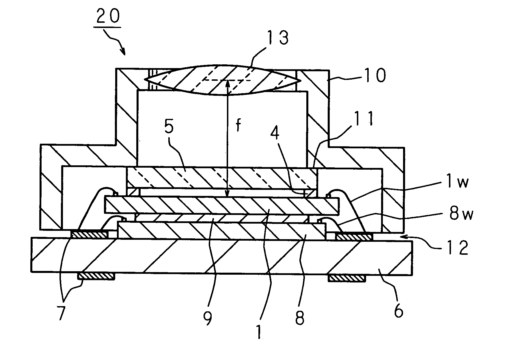
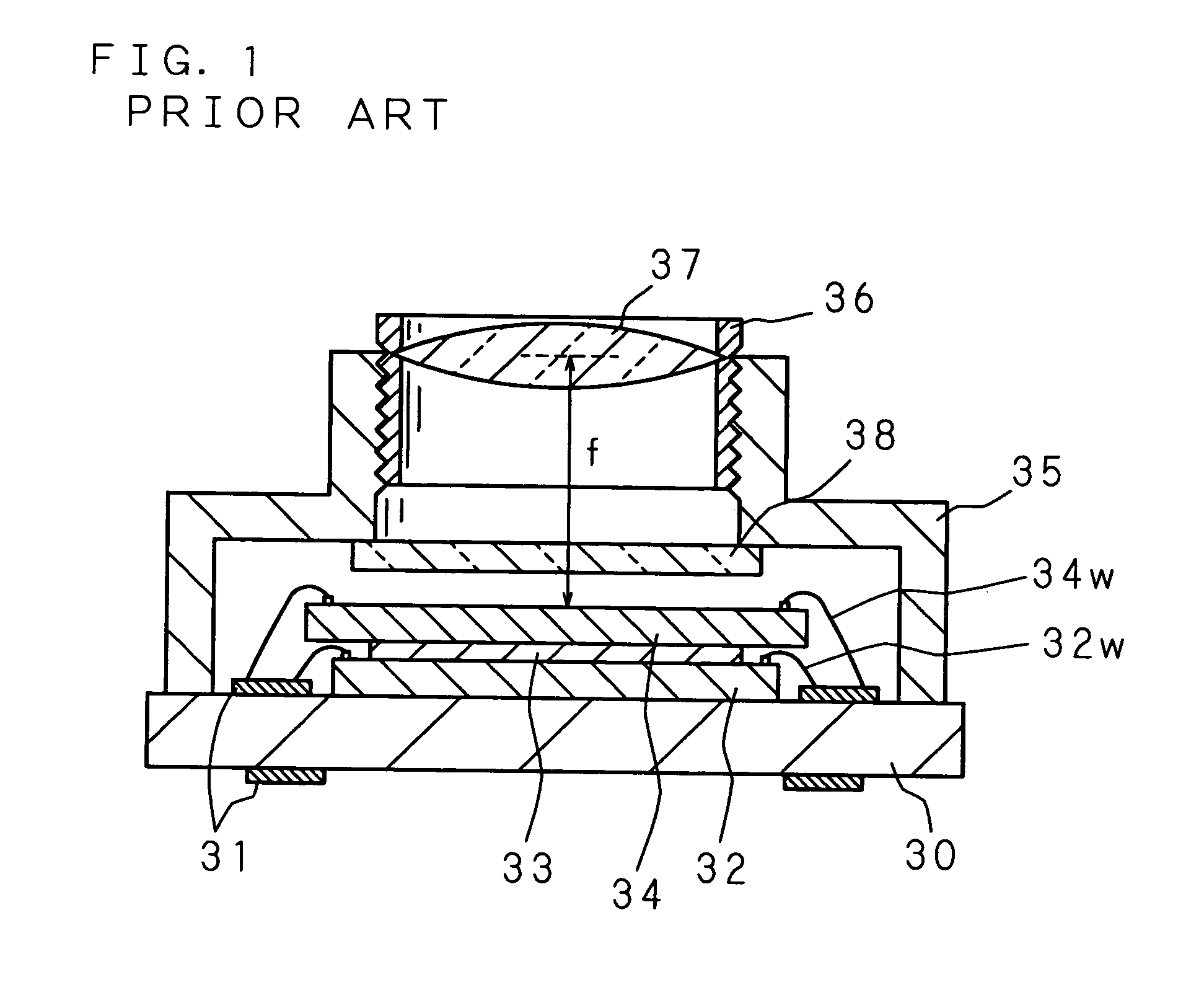
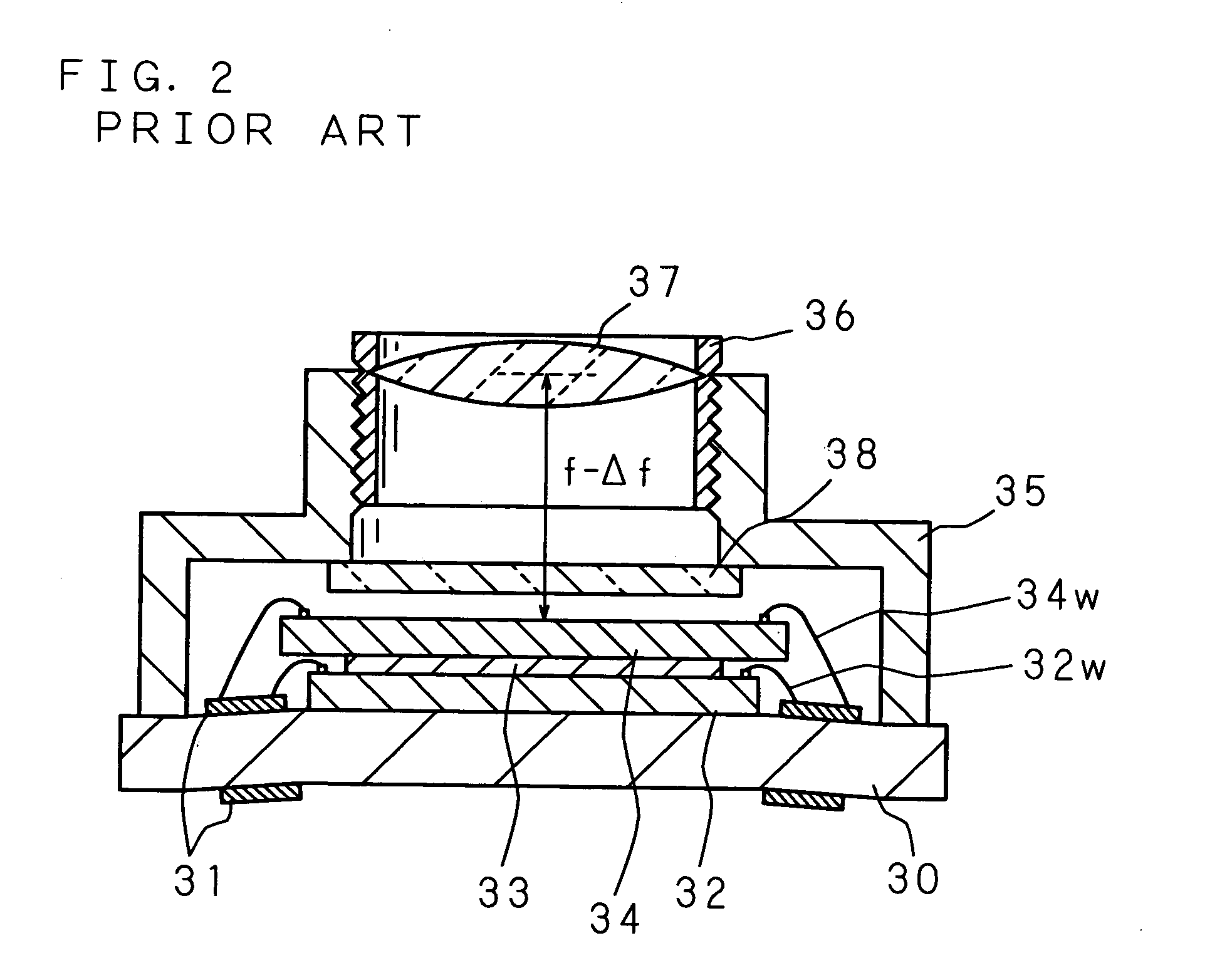
[0049]A module for an optical device according to the invention will be described below with reference to drawings showing its preferred embodiment.

[0050]FIG. 5 is a schematic plan view showing a plane shape of a solid-state image sensor, according to a first constructional example, used in a module for an optical device according to the invention. FIG. 6 is a schematic sectional view taken along line A—A in FIG. 5. Reference numeral 1 denotes the solid-state image sensor which is formed on a semiconductor substrate such as silicon with a semiconductor processing technique. An effective pixel region 2 for performing a photoelectric conversion is formed at the center portion of one side (the surface on which a lens 13 described later is placed: this surface will be hereinafter referred to as an upper surface) of the solid-state image sensor 1. Formed at the peripheral portion of the solid-state image sensor 1 are bonding pads 3 that are connecting terminals for establishing a connect...


PUM


Abstract

A module for an optical device being provided with a wiring substrate having a conductive wiring patterned thereon, a solid-state image sensor, a DSP for controlling the operation of the solid-state image sensor and processing a signal outputted from the same, and a lens holder being placed opposite to the solid-state image sensor and having a function of an optical path demarcating unit for demarcating the optical path to the solid-state image sensor, wherein a transparent cover bonded to the surface of the solid-state image sensor is joined to the lens holder at a joint portion. It is unnecessary to provide a focus adjuster for matching the optical distance between the lens and the solid-state image sensor with the focal length of the lens.

Description

CROSS-REFERENCE TO RELATED APPLICATIONS[0001]This Nonprovisional application claims priority under 35 U.S.C. §119(a) on Patent Application No. 2003-092329 filed in Japan on Mar. 28, 2003, the entire contents of which are hereby incorporated by reference.BACKGROUND OF THE INVENTION[0002]1. Field of the Invention[0003]The invention relates to a module for an optical device suitable for a camera module and the like for capturing an image of an object, and to a manufacturing method therefor.[0004]2. Description of Related Art[0005]A portable electronic apparatus such as a cellular phone or the like has recently been equipped with a camera function, so that a module for an optical device such as a camera module has been developed (for example, see Japanese Patent Application Laid-Open No. 2002-182270).[0006]FIG. 1 is a schematic view showing a section of a conventional module for an optical device. Reference numeral 30 denotes a wiring substrate 30 which has conductive wirings 31 pattern...

Claims


Application Information

Patent Timeline
Patent Type & Authority Patents(United States)
IPC IPC(8): H01L31/0203H01L31/062G02B7/02H01L23/02H01L25/065H01L25/07H01L25/18H01L27/14H01L27/146H04N5/225
CPCG02B7/02H01L27/14618H01L27/14625H04N5/2253H01L2224/48091H01L2224/48227H01L2924/09701H01L2924/3025H01L2924/00014H01L2924/00H04N23/54G03B30/00
Inventor TSUKAMOTO, HIROAKIFUJITA, KAZUYAYASUDOME, TAKASHI
Owner SHARP KK
Why Eureka
Try Eureka