Test circuit provided with built-in self test function

a test circuit and self-testing technology, applied in the field of test circuits, can solve the problems of increasing equipment cost, disadvantage and inconvenience, and the inability to test sdram so far

Active Publication Date: 2006-09-26
LAPIS SEMICON CO LTD
View PDF6 Cites 37 Cited by
  • Summary
  • Abstract
  • Description
  • Claims
  • Application Information

AI Technical Summary

Problems solved by technology

That is, in cases where the high-speed SDRAM is intended to be tested by the conventional BISI circuit with the actual operating frequency exceeding the test clock, the SDRAM can not be tested so far.
However, the speeding up of the semiconductor integrated circui

Method used


Image

  • Test circuit provided with built-in self test function
  • Test circuit provided with built-in self test function
  • Test circuit provided with built-in self test function

Examples


first embodiment

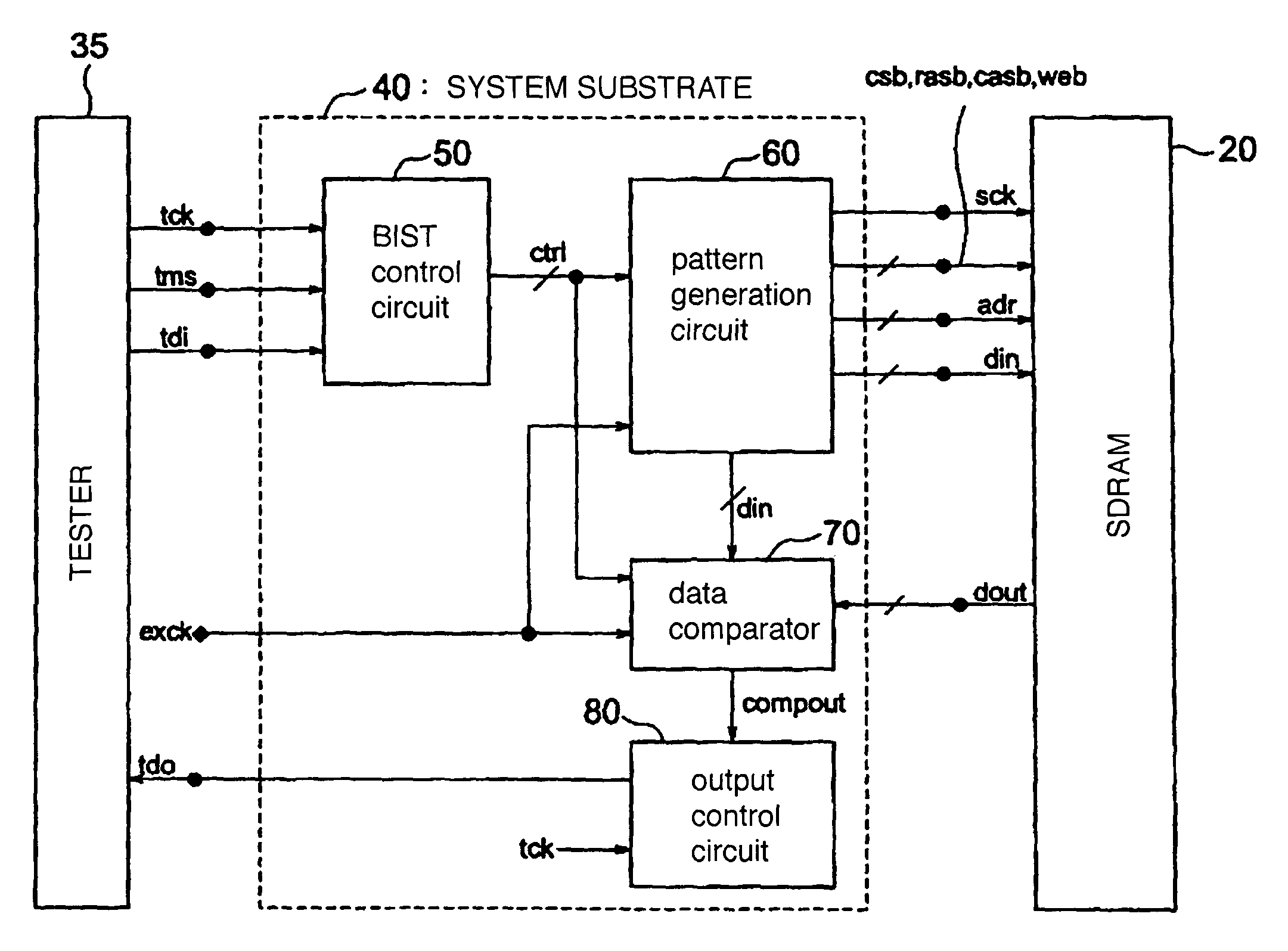
[0020]FIG. 1 is schematic circuit diagram showing a structure of a circuit (e.g., a BIST circuit) according to the invention.

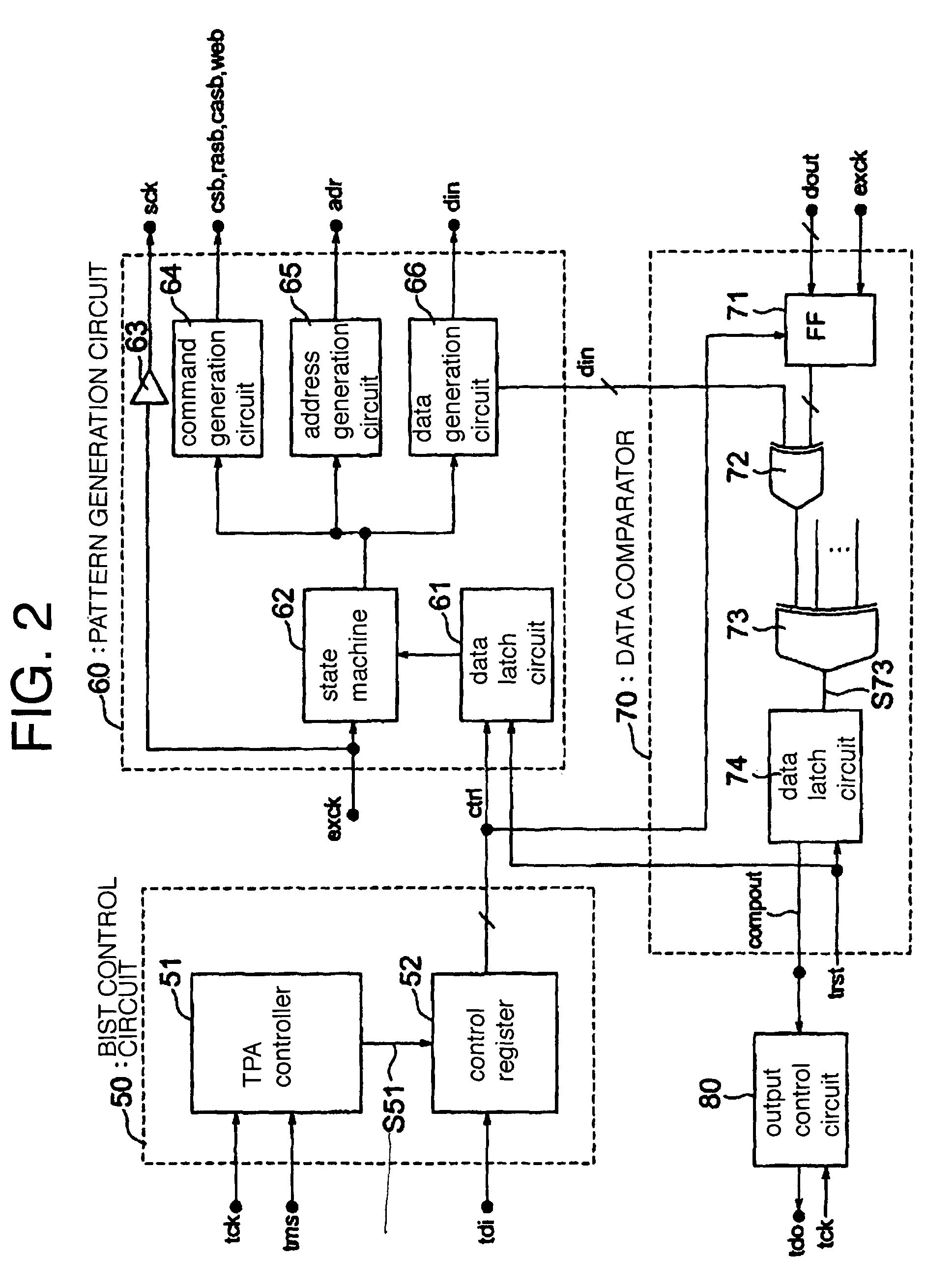
[0021]A BIST circuit 40 is a circuit for testing a circuit to be tested (e.g., an SDRAM 20 serving as a semiconductor memory) using a conventional tester 35 and has input means (e.g., a BIST control circuit 50), pattern generation means (e.g., pattern generation circuit 60) and comparator means (e.g., data comparator 70) which are connected to an output of input means, respectively. Further, output means (e.g., output control circuit 80) is connected to an output of the data comparator 70. These BIST control circuit 50, pattern generation circuit 60, data comparator 70 and output control circuit 80 are formed, e.g., on the same semiconductor substrate.

[0022]The BIST control circuit 50 inputs data for selecting a test mode relative to the SDRAM 20 (data for a standard serial interface in compliance with a JTAG standard, e.g., a test clock tck serving as a first...

second embodiment

[0054]As shown in FIG. 6, the pattern generation circuit 60A of the second embodiment is structured to have a circuit for outputting the test pattern end signal testend (e.g., a logic circuit 67) is newly provided in the pattern generation circuit 60 shown in FIG. 2. The logic circuit 67 detects the end of a test pattern while executing logical operation between an output of the command generation circuit 64 and an output of an address generation circuit 65, and outputs the test pattern end signal testend to an external tester 35 and the like.

[0055]Other configurations of the second embodiment are the same as those of the first embodiment.

[0056]FIG. 7 shows a waveform chart showing waveforms representing an example of testing the SDRAM 20 using the BIST circuit 40A in FIG. 5. According to this waveform chart, an example of reading operation of the SDRAM 20 is illustrated in the same way as FIG. 4 showing waveforms of the first embodiment.

[0057]Test date is first written in the SDRAM...

third embodiment

[0077]The third embodiment has the following effects.

[0078]Since the oscillator 111 for generating the external clock exck which is different group of the test clock tck is provided in the control chip 110, the SDRAM 20 and logic circuit 112 can be independently controlled. Accordingly, the SDRAM 20 and logic circuit 112 can be tested parallelly. It is possible to supply a specific frequency to the SDRAM 20 and to supply various frequencies to the logic circuit 112 during the parallel test. Accordingly, it is expected to shorten a test time significantly.

[0079]Since it is structured that the test pattern end signal testend can be outputted from the control chip 110, a complex control can be easily made by the tester 35 during the parallel test.

[0080]FIG. 10 is a schematic circuit diagram showing an example of a structure of a semiconductor integrated circuit (e.g., system substrate) showing a fourth embodiment of the invention on which the BIST circuit 40A of the second embodiment s...


PUM


Abstract

A test circuit includes an input circuit for inputting data to select a test mode relative to a circuit to be tested and outputting result of selection of the test mode in synchronization with a first clock, a pattern generation circuit for responding to result of selection of the test mode, generating a test pattern in synchronization with a second clock and outputting the test pattern to the circuit to be tested and a comparator circuit for inputting result of test of the circuit to be tested in synchronization with the second clock, and comparing coincidence/non-coincidence between the result of the test and the test pattern supplied to the circuit to be tested. The test circuit further includes an output circuit for holding result of comparison by the comparator circuit and outputting the result of comparison in synchronization with the first clock.

Description

BACKGROUND OF THE INVENTION[0001]The invention relates to a test circuit such as a built-in self test (hereinafter referred to as BIST) circuit and the like provided with two group of clocks which are different in frequency for testing a circuit to be tested such as a high-speed semiconductor memory and the like, and a semiconductor integrated circuit such as a control chip, a system large scaled integrated circuit (hereinafter referred to as system LSI) and the like, in which the test circuit is built in, and a method of testing the same.[0002]A technology relating to a conventional BIST serving as one of test circuits for testing a semiconductor integrated circuit and the like has been disclosed in JP-A H10-199294, JP-A 2002-174662.[0003]The BIST circuit is a circuit for generating commands of a circuit to be tested (e.g., Synchronous Dynamic Random Access Memory serving as one of semiconductor memories, hereinafter referred to as “SDRAM”), and it is used, for example, when connec...

Claims


Application Information

Patent Timeline
IPC IPC(8): G06F11/00G01R31/317G01R31/28G01R31/3187G01R31/319G11C29/02G11C29/12
CPCG01R31/31723G01R31/31725G01R31/31926G01R31/31921G01R31/3187
Inventor YONAGA, TAKERUFUKUYAMA, HIROYUKITANAKA, HITOSHI
Owner LAPIS SEMICON CO LTD
Why Eureka
Try Eureka