SO2 treatment of oxidized CuO for copper sulfide formation of memory element growth

Active Publication Date: 2006-10-03
MONTEREY RES LLC
View PDF10 Cites 8 Cited by
  • Summary
  • Abstract
  • Description
  • Claims
  • Application Information

AI Technical Summary

Benefits of technology

[0009]The present invention provides organic memory devices containing organic memory cells having a CuS layer formed by an SO2 treatment of a copper oxide surface, such as an oxidized surface of a copper containing electrode. Consequently, the thickness of the CuS layer is relatively small and controllable, compared with forming CuS layers by other methods. The use of dangerous compounds to form a CuS layer, such as H2S, is mitigated and/or eliminated. Moreover, since the CuS layer may be formed within an electrode, delaminat

Problems solved by technology

However, silicon-based devices are approaching their fundamental physical size limits.
Inorganic solid state devices are generally encumbered with a complex architecture which leads to high cost and a loss of data storage density.
The circuitry of volatile semiconductor memories based on inorganic semiconductor material must constantly be supplied with electric current with a resulting heating and high electric power consumption in order to maintain stored information.
Non-volatile semiconductor devices have a reduced data rate and relatively high power consumption and large degree of complexity.
Moreover, as inorganic solid state device sizes decrease and integration increases, sensitivity to alignment tolerances increase

Method used


Image

  • SO2 treatment of oxidized CuO for copper sulfide formation of memory element growth
  • SO2 treatment of oxidized CuO for copper sulfide formation of memory element growth
  • SO2 treatment of oxidized CuO for copper sulfide formation of memory element growth

Examples


Example

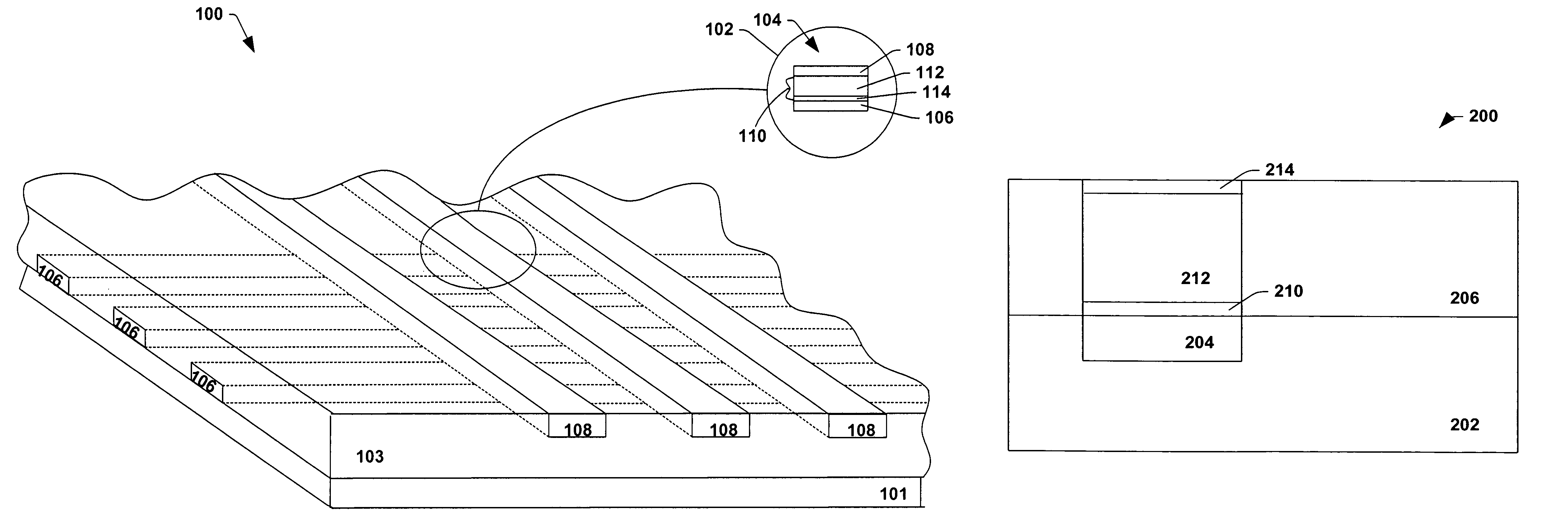
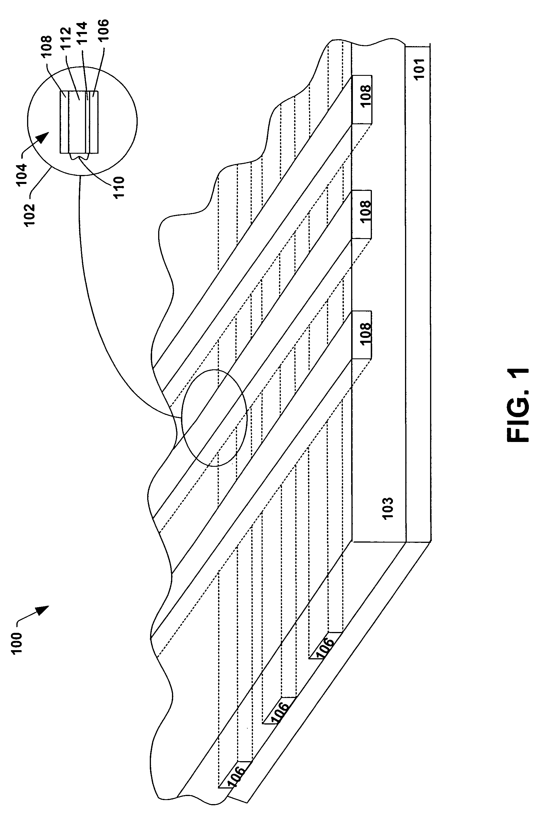
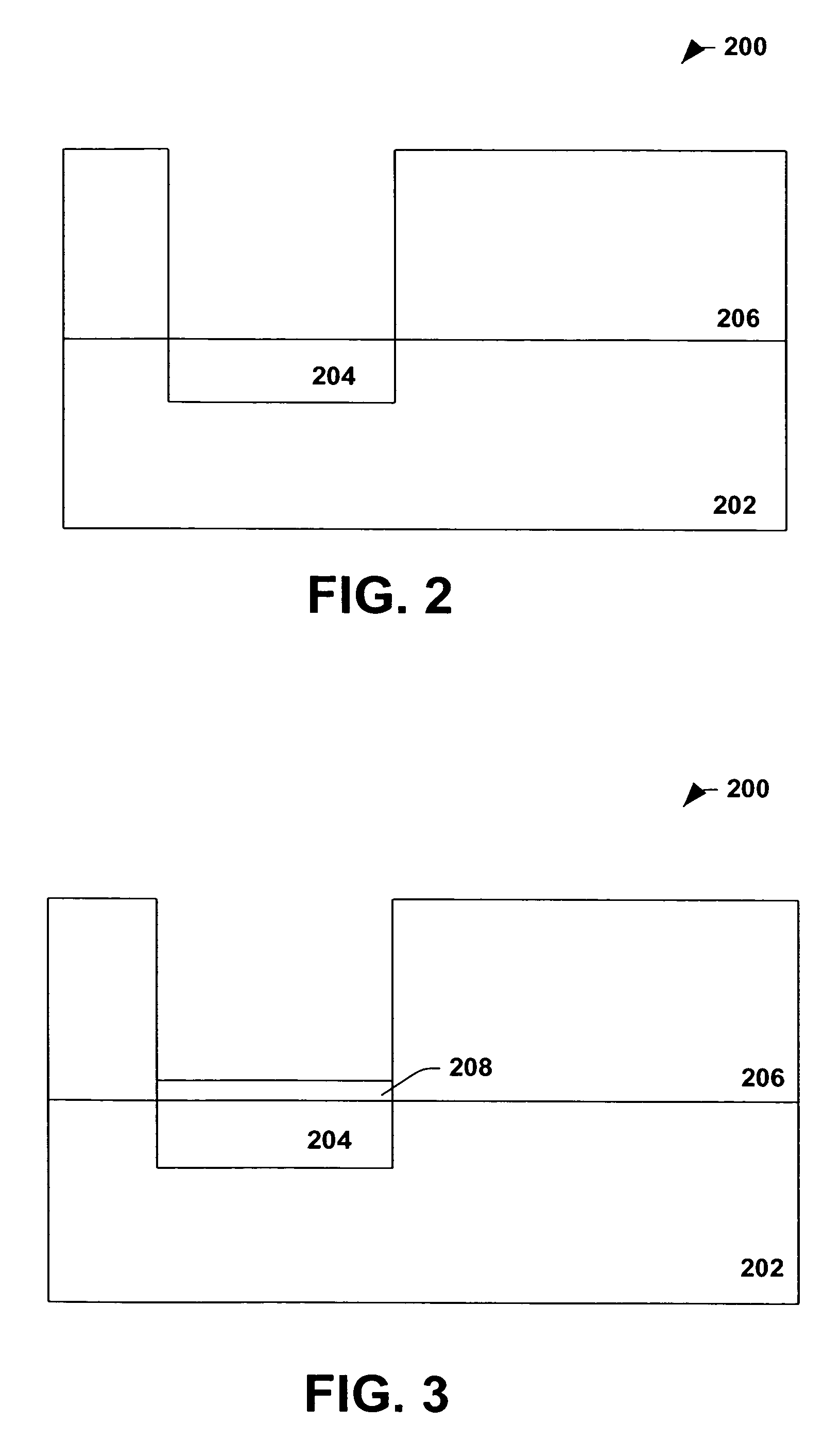
[0018]The present invention involves using a sulfur treatment to form CuS layers or regions in organic memory cells made of two electrodes with a controllably conductive media between the two electrodes. The controllably conductive media contains an organic semiconductor layer and the CuS layer, the latter formed by the sulfur treatment of an oxidized surface. Specifically, copper in an electrode is oxidized to form copper oxide, than the copper oxide is efficiently converted to copper sulfide. The organic memory cells may optionally contain additional layers, such as additional electrodes, charge retention layers, and / or chemically active layers.

[0019]The impedance of the controllably conductive media changes when an external stimulus such as an applied electric field is imposed. A plurality of organic memory cells, which may be referred to as an array, form an organic memory device. In this connection, organic memory cells may form an organic memory device and function in a manner...


PUM


Abstract

Disclosed are methods of making memory cells and semiconductor devices containing the memory cells. The methods involve oxidizing a portion of a copper containing electrode to form a copper oxide layer; contacting the copper oxide layer with at least one of a sulfur containing gas or plasma to form a CuS layer; forming an organic semiconductor over the CuS layer; and forming an electrode over the organic semiconductor. Such devices containing the memory cells are characterized by light weight and robust reliability.

Description

TECHNICAL FIELD[0001]The present invention generally relates to using a gaseous treatment to form passive layers in organic memory devices. In particular, the present invention relates to CuS passive layers formed by an SO2 treatment in memory devices containing an organic semiconductor.BACKGROUND ART[0002]The basic functions of a computer and memory devices include information processing and storage. In typical computer systems, these arithmetic, logic, and memory operations are performed by devices that are capable of reversibly switching between two states often referred to as “0” and “1”. Such switching devices are fabricated from semiconducting devices that perform these various functions and are capable of switching between two states at high speed.[0003]Electronic addressing or logic devices, for instance for storage or processing of data, are made with inorganic solid state technology, and particularly crystalline silicon devices. The metal oxide semiconductor field effect t...

Claims


Application Information

Patent Timeline
IPC IPC(8): H01L21/00
CPCB82Y10/00G11C13/0014G11C13/0016H01L51/0575G11C2213/77H01L27/285H01L51/105H10K19/202H10K10/20H10K10/84
Inventor LYONS, CHRISTOPHER F.SUBRAMANIAN, RAMKUMARLOPATIN, SERGEY D.XIE, JAMES J.HUI, ANGELA T.
Owner MONTEREY RES LLC
Why Eureka
Try Eureka