Bypass capacitor embedded flip chip package lid and stiffener

a bypass capacitor and flip chip technology, applied in the direction of electrolytic capacitors, printed circuit non-printed electric components association, electrical apparatus contruction details, etc., can solve the problems of less reliable the flip chip package becomes, the flip chip package may experience some degree of simultaneous switching noise (ssn), and the operation of die errors, so as to control the simultaneous switching noise and minimize ssn. , the effect of instant power

Inactive Publication Date: 2006-10-03
ALTERA CORP
View PDF6 Cites 56 Cited by
  • Summary
  • Abstract
  • Description
  • Claims
  • Application Information

AI Technical Summary

Benefits of technology

[0008]To achieve the foregoing, the present invention provides a heat spreader with an embedded bypass capacitor to provide substantially instant power and / or to control simultaneous switching noise (SSN). The present invention also provides a semiconductor device package incorporating this heat spreader. In addition, fabrication methods for such heat spreaders and packages are provided. Generally, the heat spreaders and packages of the present invention include an embedded bypass capacitor that can provide decoupling capacitance in order to deliver near instant power to the die and / or minimize SSN.

Problems solved by technology

Since the system power supply is often located a substantial distance away from the flip chip package, a long time delay and large inductance associated with the power and ground leads are introduced into the flip chip package's power delivery system.
During its operation, a flip chip package may experience some degree of simultaneous switching noise (SSN).
As a result, SSN may cause errors in the operation of the die (e.g., drivers not responding correctly).
Therefore, the more SSN present, the less reliable the flip chip package will become.

Method used


Image

  • Bypass capacitor embedded flip chip package lid and stiffener
  • Bypass capacitor embedded flip chip package lid and stiffener
  • Bypass capacitor embedded flip chip package lid and stiffener

Examples


first embodiment

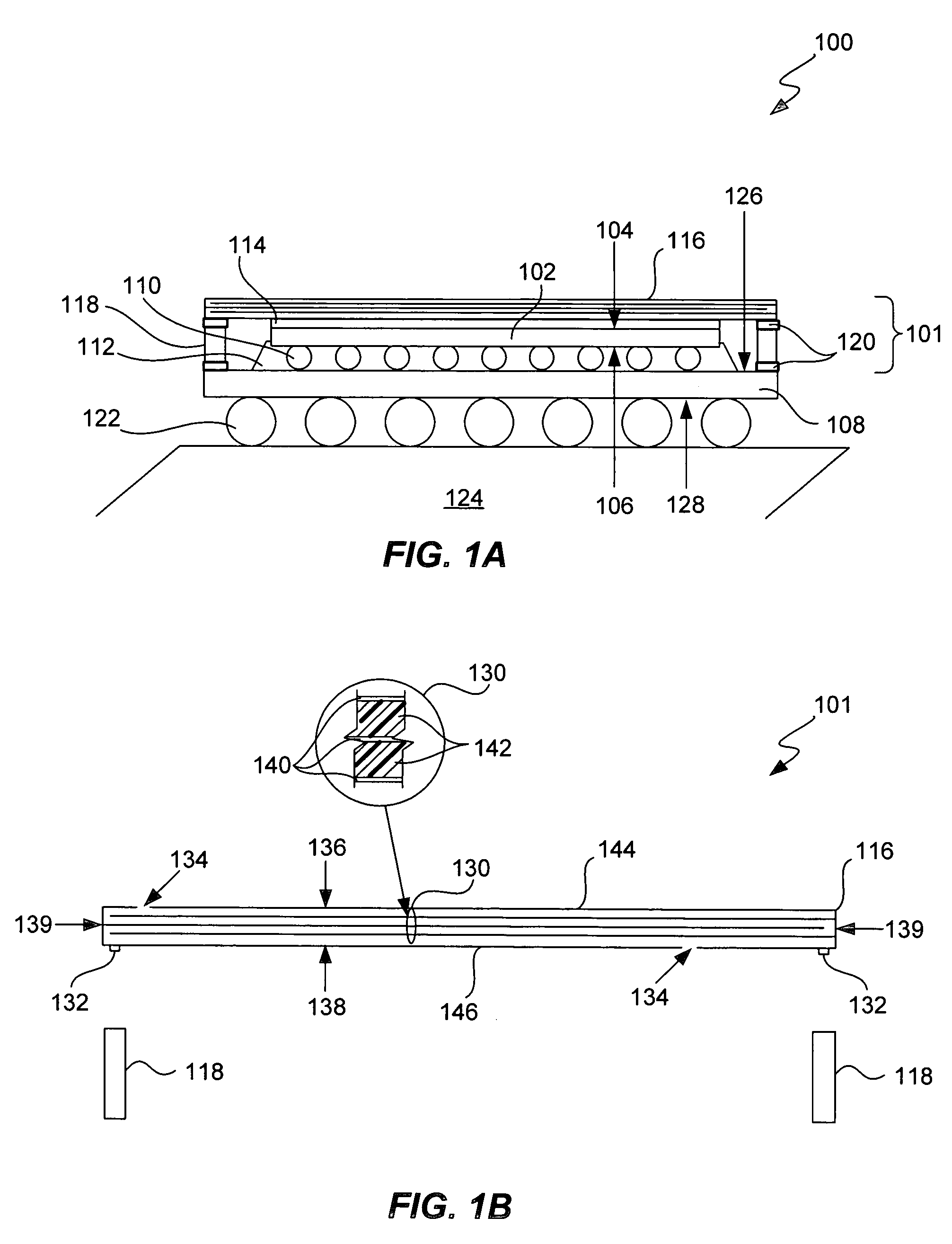
[0032]A variety of strategies are used in providing near instant power and / or minimizing SSN. For example, FIG. 1A illustrates a cross-sectional view of a semiconductor device package according to the present invention. As shown, flip chip package 100 includes a die 102 having a front surface 106 (i.e., active surface) and a back surface 104 (i.e., inactive surface). Die 102 may have any suitable set of dimensions. In one example, die 102 may have dimensions on the order of about 100–1089 mm2 and 12–32 mils thick.

[0033]Once die 102 is chosen, die 102 is attached to a corresponding flip chip package substrate 108. Package substrate 108 may also have any suitable set of dimensions. For example, package substrate 108 may have dimensions on the order of about 400–2025 mm2 (e.g., 23×23 mm, 45×45 mm). In attaching die 102 to package substrate 108, die 102 is positioned over package substrate 108 and bonded electrically and mechanically together in a solder joining operation. As shown, fli...

second embodiment

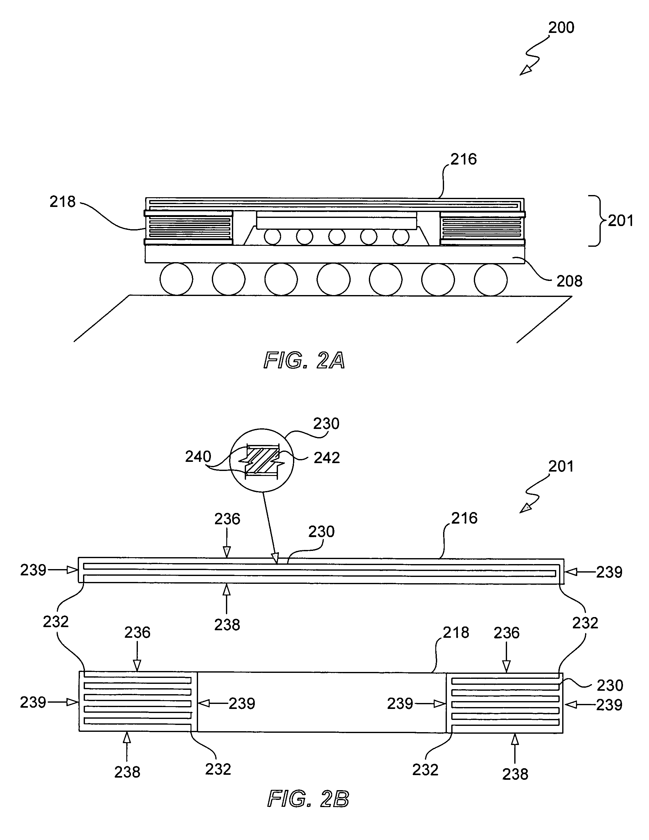
[0043]Next, FIG. 2A illustrates a cross-sectional view of a semiconductor device package according to the present invention. Many of the flip chip package processes and flip chip package elements used in flip chip package 100 may be used in flip chip package 200. As shown, a bypass capacitor embedded heat spreader 201 is used to form flip chip package 200.

[0044]To elaborate on bypass capacitor embedded heat spreader 201, reference will now be made to FIG. 2B. Bypass capacitor embedded heat spreader 201 (e.g., lid 216; stiffener 218) has a top surface 236, a bottom surface 238, and a plurality of side surfaces 239 that surrounds a bypass capacitor 230. The stiffener (also sometimes referred to as a “picture frame” or “window frame” due to the stiffener's appearance) is typically a flat piece of metal about 10 to 40 mils thick, having substantially the same dimensions as the package substrate with a window opening in its center to clear the die. One of the purposes of a stiffener is t...

third embodiment

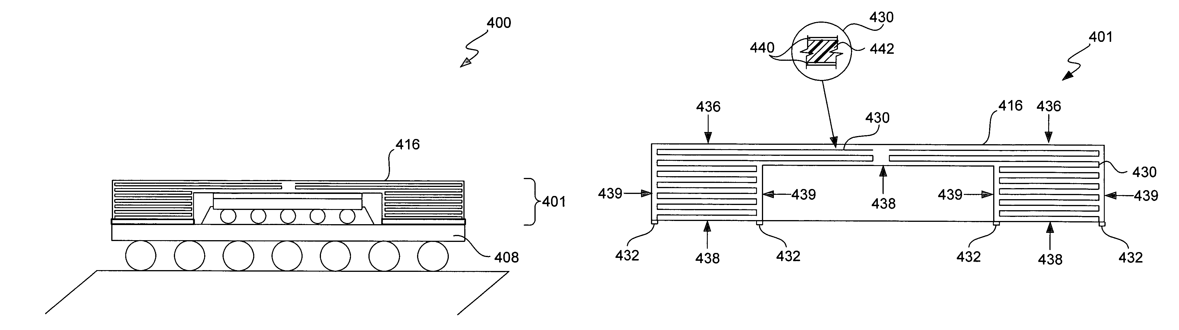
[0049]Next, FIG. 3A illustrates a cross-sectional view of a semiconductor device package according to the present invention. Many of the flip chip package processes and flip chip package elements used in flip chip package 100 may be used in flip chip package 300. As shown, a bypass capacitor embedded heat spreader 301 is used to form flip chip package 300. Bypass capacitor embedded heat spreader 301 is a one-piece heat spreader construction with leg openings at two opposite ends. The openings allow for heat spreader 301 to accommodate a die that extends beyond the open ends and, typically, beyond the corresponding edges of package substrate 308. This type of heat spreader is commonly known as a channel type lid.

[0050]To elaborate on bypass capacitor embedded heat spreader 301, reference will now be made to FIG. 3B. Bypass capacitor embedded heat spreader 301 (e.g., lid 316) has a top surface 336, a plurality of bottom surfaces 338, and a plurality of side surfaces 339 that surrounds...


PUM


Abstract

The present invention provides a heat spreader with a bypass capacitor to provide substantially instant power and/or to control simultaneous switching noise (SSN). The present invention also provides a semiconductor device package incorporating this heat spreader. In addition, fabrication methods for such heat spreaders and packages are provided. Generally, the heat spreaders and packages of the present invention include an embedded bypass capacitor that can provide decoupling capacitance in order to deliver near instant power to the die and/or minimize SSN. In a preferred embodiment, the embedded bypass capacitor is connected to terminals integrated with the heat spreader (e.g., lid; stiffener) and/or to a package plane (e.g., power plane or ground plane) in the package substrate for connection via the flip chip package's power delivery system to a power source and/or component.

Description

BACKGROUND OF THE INVENTION[0001]1. Field of the Invention[0002]This invention relates generally to semiconductor device packages, and in particular to flip chip packages. More specifically, the invention relates to heat spreaders embedded with a bypass capacitor and their corresponding methods of fabrication.[0003]2. Description of the Prior Art[0004]In a semiconductor device package, a semiconductor chip (also referred to as an integrated circuit (IC) chip or “die”) may be bonded directly to a package substrate. Such a die is formed with ball-shaped beads or bumps of solder affixed to its I / O bonding pads. During packaging, the die is “flipped” onto its front surface (e.g., active surface) so that the bumps form electrical connections between the die and conductive metal pads on a package substrate. A semiconductor device package of this type is commonly called a “flip chip package”. As used herein, a flip chip package may include the packaging, the die, and / or their corresponding...

Claims


Application Information

Patent Timeline
Patent Type & Authority Patents(United States)
IPC IPC(8): H01L23/58H01L23/02H01L23/34H01L23/367H01L23/64
CPCH01L23/04H01L23/36H01L23/50H01L23/642H01L21/563H01L23/49816H01L2224/73253H01L2924/01078H01L2924/01079H01L2924/15311H01L2924/16152H01L2924/16195H01L2924/19041H01L2924/3011H01L2924/01322H01L2224/16225H01L2224/32225H01L2224/73204H01L2924/00H01L2924/10253H01L2924/00011H01L2924/00014H01L2224/0401
Inventor HOOL, VINCENT
Owner ALTERA CORP
Why Eureka
Try Eureka