Method of forming insulating layer and method of fabricating thin film transistor using the same

Active Publication Date: 2006-10-10
LG DISPLAY CO LTD
View PDF11 Cites 8 Cited by
  • Summary
  • Abstract
  • Description
  • Claims
  • Application Information

AI Technical Summary

Benefits of technology

[0022]An object of the present invention is to provide a method of forming an insulating laye

Problems solved by technology

However, amorphous silicon has a low mobility, which adversely affects the operation of a wide-screen TFT-LCD.
However, the rectangular dimensions or step profile of an etched contact hole is degraded.
Thus, a poor step profile or large diameters for each of the contact holes to a polysilicon thin film transistor increases the si

Method used


Image

  • Method of forming insulating layer and method of fabricating thin film transistor using the same
  • Method of forming insulating layer and method of fabricating thin film transistor using the same
  • Method of forming insulating layer and method of fabricating thin film transistor using the same

Examples


Example

[0034]Reference will now be made in detail to the preferred embodiments of the present invention, examples of which are illustrated in the accompanying drawings. Wherever possible, the same reference numbers will be used throughout the drawings to refer to the same or like parts.

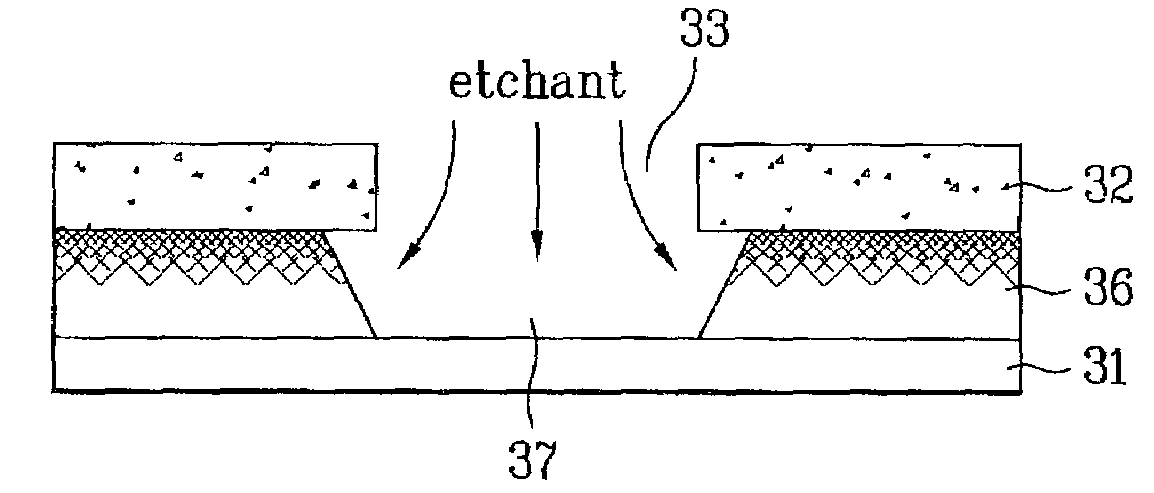
[0035]FIG. 3 illustrates a cross-sectional view for a method of forming an insulating layer according to one embodiment of the present invention. When an insulating layer 36, as shown in FIG. 3, is deposited on a glass substrate 31, a gas composition ratio, RF strength, pressure and temperature inside a vacuum chamber, and the distance between upper and lower electrodes are varied to control a density of the insulating layer 36. For example, the gas composition ratio on the glass substrate 31, as shown in FIG. 3, is maintained uniformly but the RF strength, pressure, temperature, and the like are increased gradually to increase the density of the insulating layer 36 gradually as the layer is deposited. Then,...


PUM

PropertyMeasurementUnit
Temperatureaaaaaaaaaa
Pressureaaaaaaaaaa
Densityaaaaaaaaaa

Abstract

A method of forming an insulating layer including preparing a substrate and depositing an insulating layer on the substrate such that density of a top portion of the insulating layer is different from that of a bottom portion of the insulating layer.

Description

[0001]This application claims the benefit of the Korean Application No. P2001-87130 filed on Dec. 28, 2001, which is hereby incorporated by reference.BACKGROUND OF THE INVENTION[0002]1. Field of the Invention[0003]The present invention relates to a liquid crystal display device, and more particularly, to a method of forming an insulating layer to control the step profile of a hole therethrough and a method of fabricating a thin film transistor using the same.[0004]2. Discussion of the Related Art[0005]As an information society develops, so increases the demand for information displays. Recently, many efforts have been made to research and develop various flat display panels, such as a liquid crystal display (LCD), a plasma display panel (PDP), a electroluminescent display (ELD), a vacuum fluorescent display (VFD), and the like. Due to the characteristics or advantages of a high quality color image, low weight, compact size, and low power consumption, an LCD is typically used instead...

Claims


Application Information

Patent Timeline
IPC IPC(8): H01L21/84H01L21/00C23C16/30H01L29/786C23C16/44C23C16/455H01L21/311H01L21/314H01L21/316H01L21/336H01L21/768
CPCC23C16/30C23C16/45523H01L21/0214H01L21/02164H01L21/0217H01L21/022H01L21/02274H01L21/3144H01L21/3145H01L21/31612H01L29/66757H01L21/31116H01L21/76802H01L29/786
Inventor HWANG, EUI HOONPARK, CHAN IL
Owner LG DISPLAY CO LTD
Why Eureka
Try Eureka