Method of manufacturing a floating gate and method of manufacturing a non-volatile semiconductor memory device comprising the same

a semiconductor memory and floating gate technology, applied in the direction of semiconductor devices, electrical devices, transistors, etc., can solve the problems of inconvenient assembly, inconvenient operation, and inability to precisely align the gates, so as to facilitate high-speed reading and writing of data without consuming a large amount of power, and enhance the efficiency of electron discharging and injecting. , the effect of high degree of integration

Inactive Publication Date: 2006-10-10
SAMSUNG ELECTRONICS CO LTD
View PDF10 Cites 8 Cited by
  • Summary
  • Abstract
  • Description
  • Claims
  • Application Information

AI Technical Summary

Benefits of technology

[0011]A feature of the present invention is to provide a method of forming a floating gate having enhanced electron discharging and injecting efficiencies.
[0012]Another feature of the present invention is to provide a method of manufacturing a non-volatile semiconductor memory device having a floating gate that is accurately aligned with a control gate.
[0013]In accordance with one aspect of the present invention, an edge portion of a conductive pattern, constituting a floating gate, is provided with a high degree of sharpness. To this end, first, a conductive layer is formed on a semiconductor substrate. Next, the conductive layer is patterned using a photolithographic process to form a conductive a pattern on the semiconductor substrate. Then, a first insulation layer is formed on a sidewall of the conductive pattern in such a way that the sharpness of the edge portion of the conductive pattern is increased. Subsequently, a second insulation layer is formed at the upper portion of the conductive pattern so that the edge portion of the conductive pattern is even further increased.
[0016]According to the present invention, the sharp edge portion of the floating gate enhances the efficiencies of electron discharging and injecting. In addition, the alignment between the floating gate and the control gate is ensured by forming the control gate using a dry etching process. Furthermore, the split gate type of flash semiconductor memory device of the present invention can be produced with a higher degree of integration than a conventional flash semiconductor memory device whose cell size is 2-Tr. Still further, the split gate type of flash semiconductor memory device of the present invention, when used in a logic circuit, facilitates a high speed reading and writing of data without consuming a large amount of power.

Problems solved by technology

Accordingly, the speed at which electrons can be transferred from the floating gate to the control gate is still rather limited.
However, in the methods described above, additional processes are required for forming the insulation layer between the floating gate and the control gate, and the gates may not be precisely aligned.
Therefore, problems still remain, such as excessive cell size and the difficulty of integrating the memory device with a logic device.

Method used


Image

  • Method of manufacturing a floating gate and method of manufacturing a non-volatile semiconductor memory device comprising the same
  • Method of manufacturing a floating gate and method of manufacturing a non-volatile semiconductor memory device comprising the same
  • Method of manufacturing a floating gate and method of manufacturing a non-volatile semiconductor memory device comprising the same

Examples


Embodiment Construction

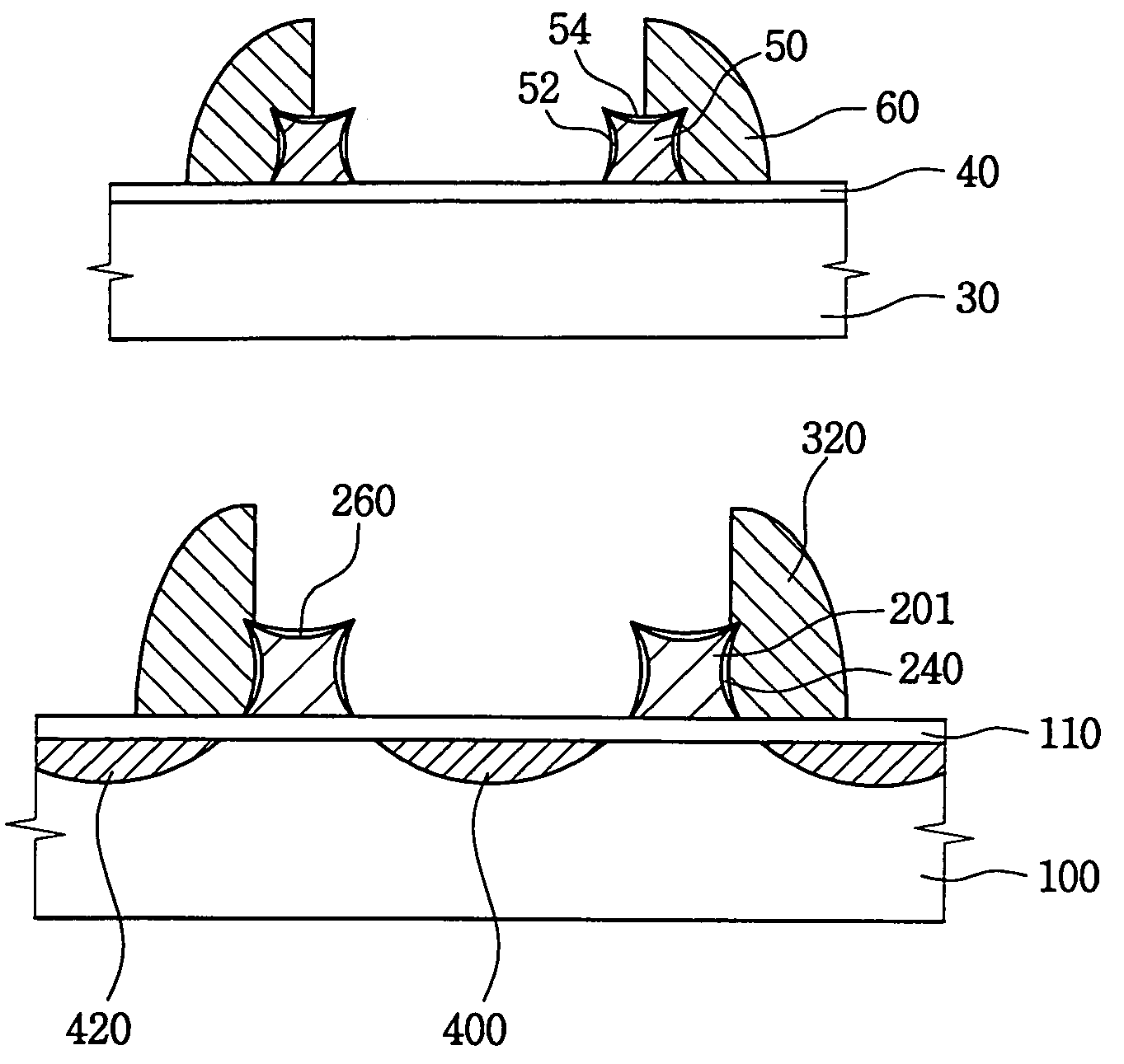
[0025]The present invention now will be described more fully hereinafter with reference to the accompanying drawings. Note, like reference numbers designate like elements throughout the drawings. Also, the relative thickness of layers may be exaggerated in the drawings for clarity in illustrating the present invention.

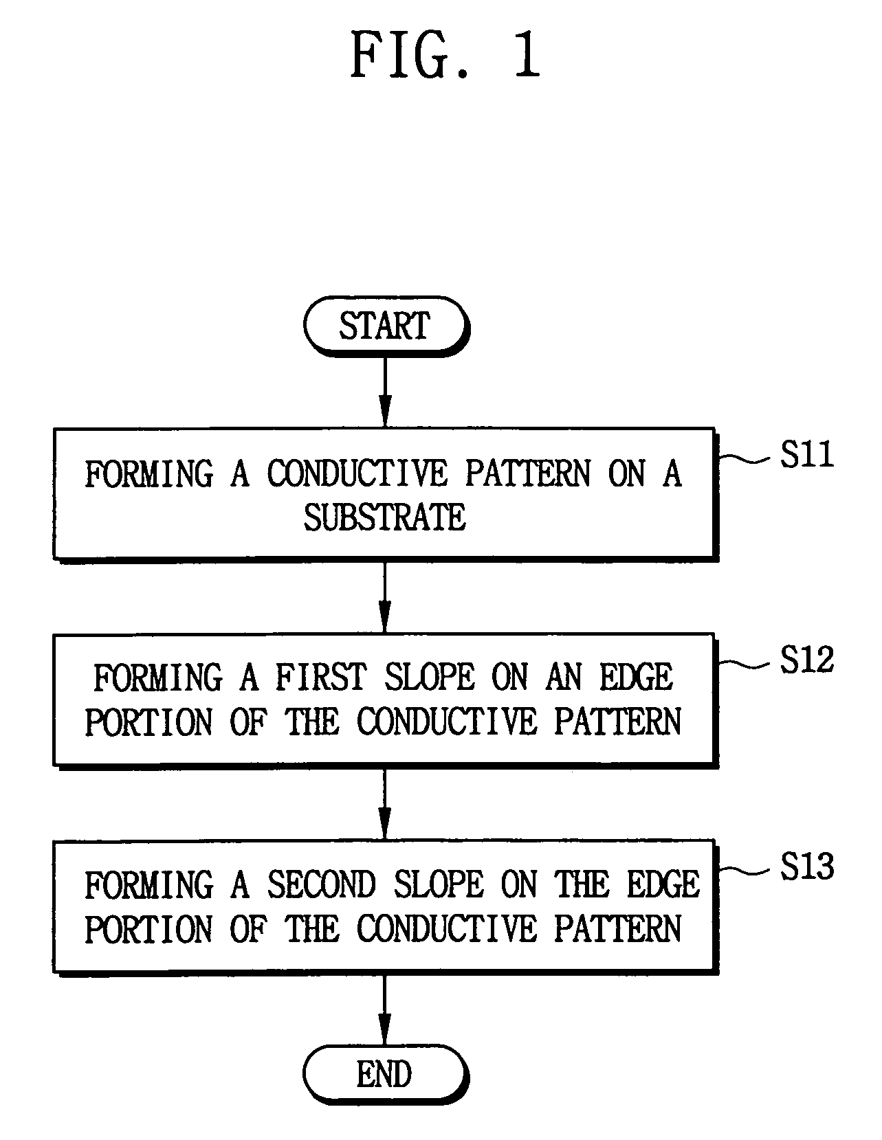
[0026]FIG. 1 outlines a first embodiment of a method of manufacturing a floating gate according to the present invention.

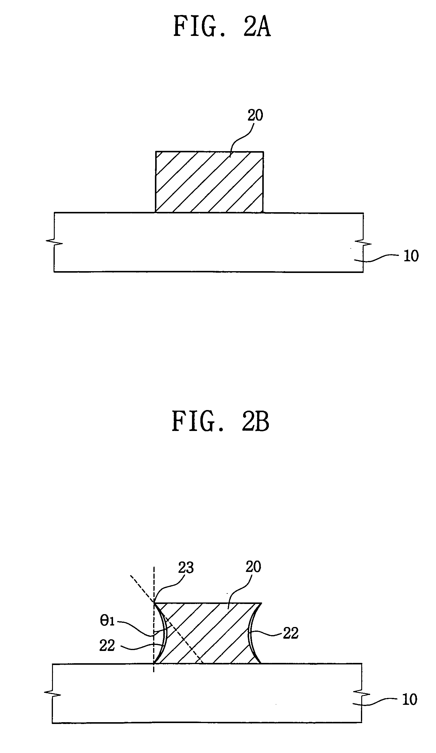
[0027]Referring to FIG. 1, a conductive layer of silicon (Si), e.g., amorphous silicon, polysilicon, or silicon doped with impurities, is formed on a semiconductor substrate (step S11). Then, the conductive layer is patterned using a photolithographic process to form a conductive pattern on the semiconductor substrate. Alternatively, the conductive layer may comprise a metal such as copper (Cu), tungsten (W), aluminum (Al), titanium (Ti), and the like.

[0028]Next, a first insulation layer is formed on a sidewall of the conductive pattern so that an ed...


PUM


Abstract

A method of manufacturing a floating gate provides an enhancement for the efficiencies of electron charge and injection. First, a conductive pattern, constituting the floating gate is formed on a substrate. A first insulation layer is formed on a sidewall of the conductive pattern, and then a second insulation layer is formed at an upper portion of the conductive pattern in ways that increase the sharpness of an edge portion where the sidewall and upper portions of the conductive pattern meet. Therefore, electron transference from the floating ate to a control gate is facilitated.

Description

BACKGROUND OF THE PRESENT INVENTION[0001]1. Field of the Present Invention[0002]The present invention relates to a method of forming a floating gate and to a method of manufacturing a non-volatile semiconductor memory device comprising a floating gate.[0003]2. Description of the Related Art[0004]Semiconductor memory devices are generally divided into volatile semiconductor memory devices and non-volatile semiconductor memory devices. In the volatile semiconductor memory device, data stored in the cell is dissipated when power is not applied. However, in the non-volatile semiconductor memory, stored data in the cell is retained even when power is not applied thereto. Because non-volatile semiconductor memory devices can store data for long periods of time, they are used to meet the current high demand for flash semiconductor memory devices such as EEPROMs (Electrically Erasable and Programmable Read Only Memories).[0005]Meanwhile, flash semiconductor memory devices can be generally c...

Claims


Application Information

Patent Timeline
Patent Type & Authority Patents(United States)
IPC IPC(8): H01L21/336H01L21/8247H01L21/28H01L21/8242H01L27/115H01L29/788H01L29/792
CPCH01L21/28273H01L27/115H01L27/11521H01L29/66825H01L29/40114H10B69/00H10B41/30
Inventor CHUNG, JIN-KUKMOON, CHANG-ROK
Owner SAMSUNG ELECTRONICS CO LTD
Why Eureka
Try Eureka