Method of forming a metal-insulator-metal capacitor in an interconnect cavity

a metal-insulator and interconnect layer technology, applied in capacitors, semiconductor devices, semiconductor/solid-state device details, etc., can solve the problems of reducing the capacitance value, reducing the thermal expansion mismatch between aluminum layer components of the interconnect layer, and ic early failure, so as to reduce the number of fabrication steps, reduce the amount of planarization, and simplify the manufacturing process

Inactive Publication Date: 2006-10-10
BELL SEMICON LLC
View PDF7 Cites 27 Cited by
  • Summary
  • Abstract
  • Description
  • Claims
  • Application Information

AI Technical Summary

Benefits of technology

[0012]The new and improved MIM capacitor of the present invention, and the method of fabricating it, are effective in overcoming the problem associated with hillock formation and its resulting detrimental impact on the capacitors formed, as well as permitting vias to be formed through the IMD insulating material to both the capacitor and the interconnect layer at substantially the same depth and dimension, allowing the IMD insulating material to assume a normal height over the capacitor preventing the formation of bulges in the IMD layer requiring extensive planarization steps to smoothen. This process also eliminates the need for additional design rules associated with interconnect pattern density equalization. The plates of the capacitor do not utilize or require the aluminum layer within the interconnect conductors, thereby avoiding the problem of thermal mismatch and hillock formation. The capacitor itself is embedded within the thickness of the conductor interconnect layer, thereby avoiding the difficulties associated with forming the capacitor above the interconnect layer in the IMD insulating material. By embedding the capacitor within the thickness of the interconnect layer, the fabrication process is simplified by reducing the amount of planarization required, reducing the number of fabrication steps connected solely with forming the capacitor, and allowing the IMD insulating material to be formed in a more uniform thickness and / or reduced thickness because the structure of the capacitor itself does not need to be accommodated in the IMD layer between the interconnect layers. This process also prevents variability in IMD thickness, resulting in a more precise interconnect delay model and in performance improvements. The reduction in IMD variability also improves IC component fabrication yield from a wafer substrate. Furthermore, because the capacitor components are embedded within the interconnect layer, the height or level of the capacitor components may be made approximately the same as the height of the interconnect layer, thereby allowing the process of forming the holes for the via interconnects through the IMD to proceed uniformly throughout the IC structure without the added risks of damaging components of different heights, as would be the case with the capacitor formed in the interlayer insulating material between the distinct interconnect layers.

Problems solved by technology

There is a relatively large thermal expansion mismatch between aluminum layer components of the interconnect layers and the interlayer insulating material.
Even if the size of the hillock is not significant enough to short the capacitor plates, the dielectric between the capacitor plates at the location of the hillock is highly stressed, increasing the leakage current, which diminishes the value of the capacitance and may eventually result in an early failure of the IC.

Method used


Image

  • Method of forming a metal-insulator-metal capacitor in an interconnect cavity
  • Method of forming a metal-insulator-metal capacitor in an interconnect cavity
  • Method of forming a metal-insulator-metal capacitor in an interconnect cavity

Examples


Embodiment Construction

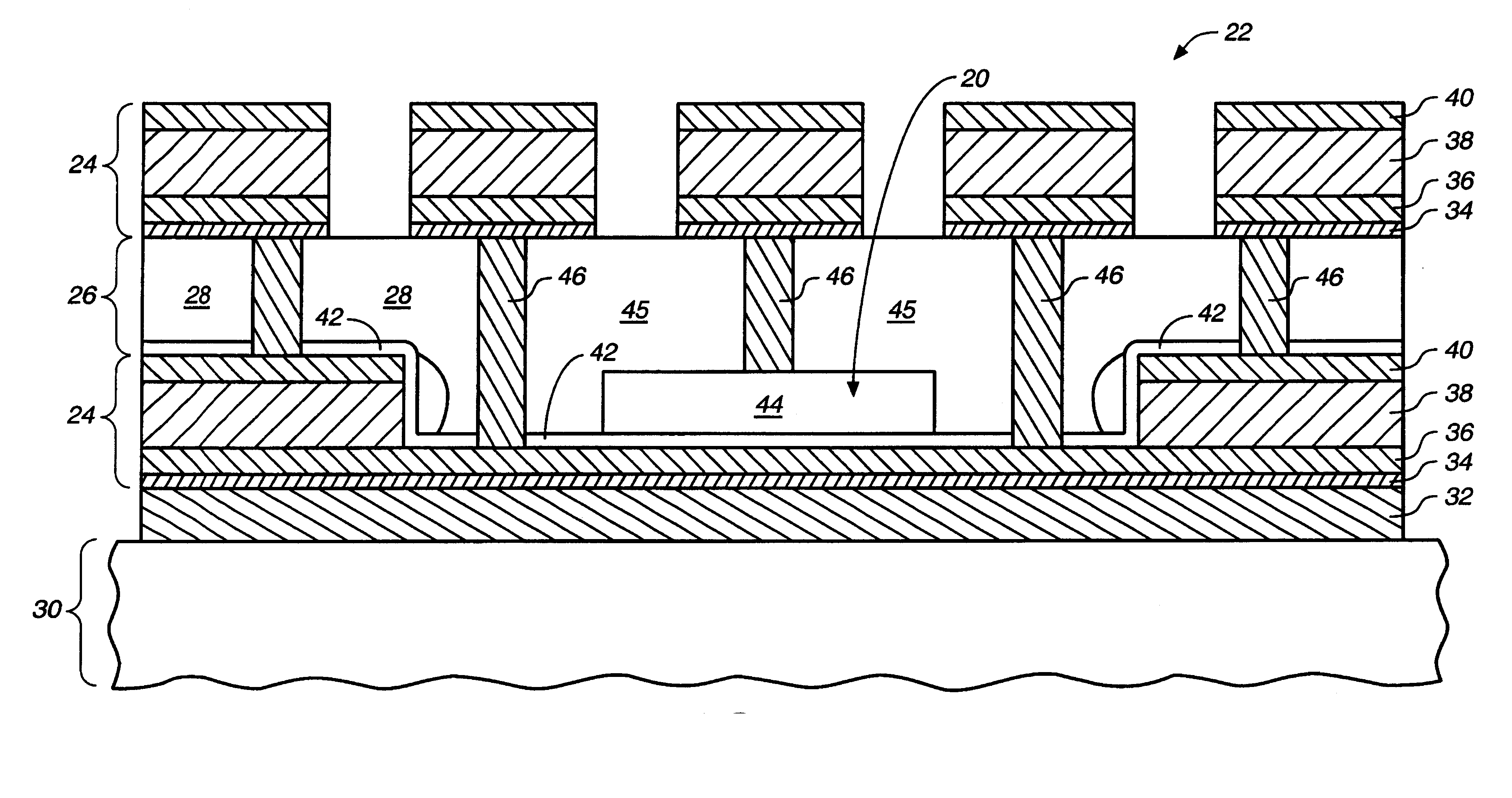
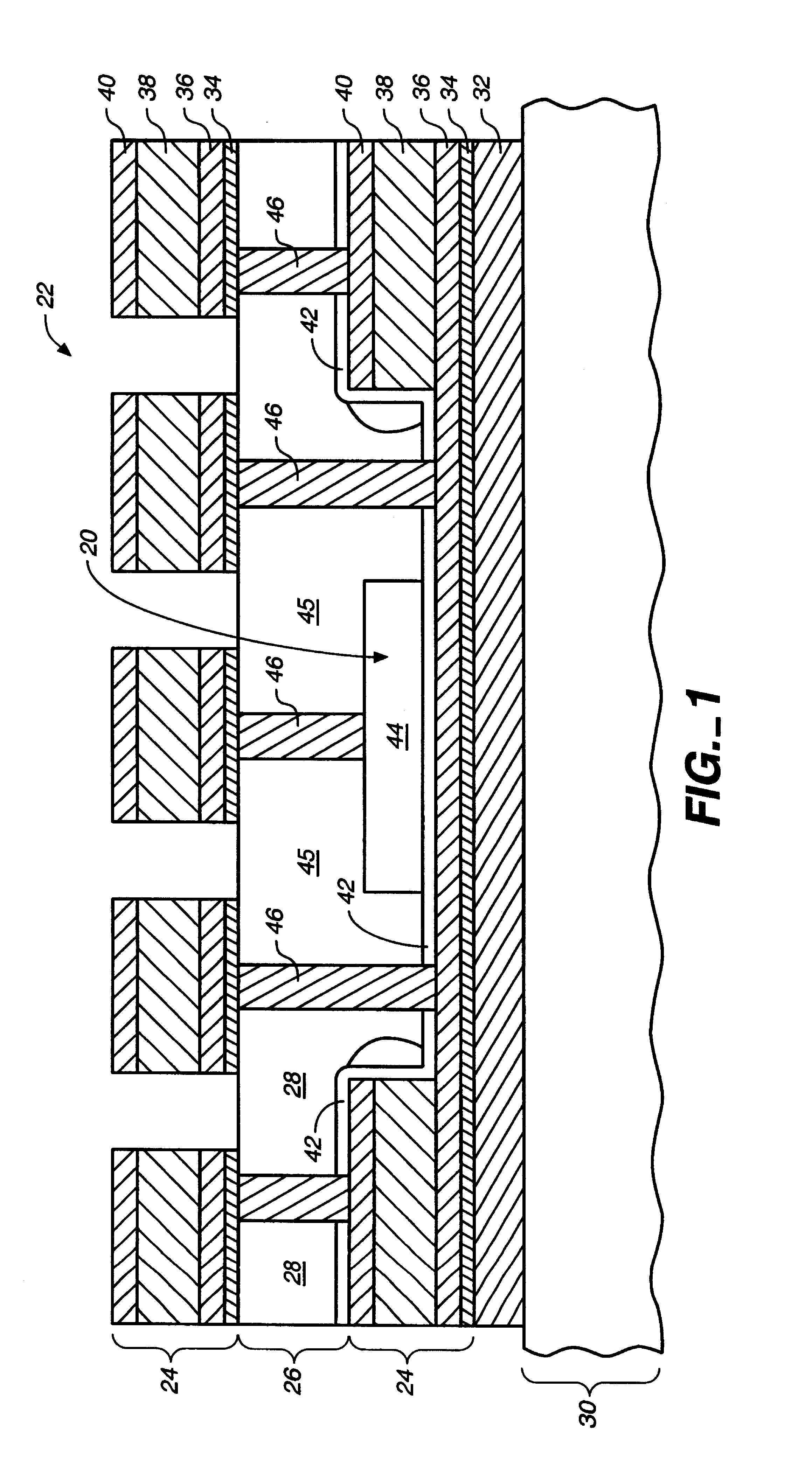
[0019]A capacitor 20 which embodies the present invention is incorporated in an integrated circuit (IC) 22 such as is shown in FIG. 1. The IC 22 is of the type having multiple layers 24 of electrical conductors known as interconnects. The electrical conductors of each interconnect layer 24 extend between and connect to the other functional components (not shown) of the IC 22. Each interconnect layer 24 is separated by a relatively thick layer 26 of interlayer dielectric (ILD) or intermetal dielectric (IMD) insulating material 28. The insulating material28 of each IMD layer 26 electrically insulates the conductors of the interconnect layers 24 from one another and electrically insulates the other components within the IC 22 from one another.

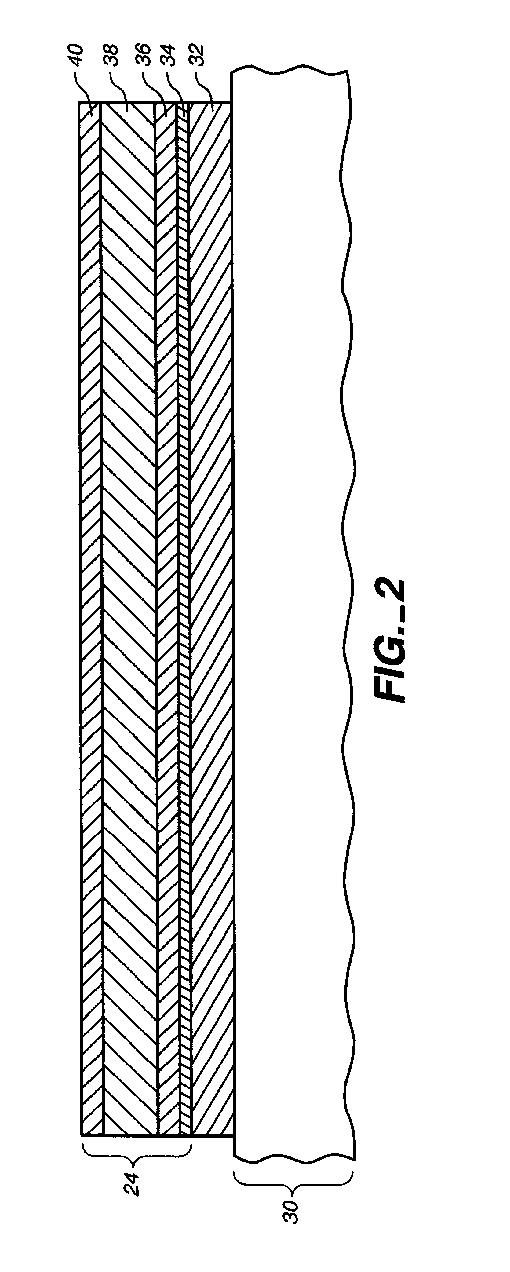
[0020]The multiple interconnect layers 24 and IMD layers 26 are built or layered above one another and overlying a substrate 30 of the IC 22. The substrate 30 serves as the foundation for the IC and its functional components formed in and on the s...


PUM


Abstract

A metal-insulator-metal capacitor is embedded in an interconnect layer of an integrated circuit (IC). The interconnect layer has a cavity, and the capacitor is formed in the cavity with one of the plates of the capacitor integral with a conductive layer of the interconnect layer, so the capacitor plate electrically communicates with the interconnect layer. The interconnect layer has multiple conductive layers, including a layer, such as aluminum, that is subject to deformation at certain temperatures during fabrication of the IC, and the cavity extends through this layer. A remaining conductive layer of the interconnect layer defines one of the capacitor plates, and a dielectric layer and another capacitor plate are formed thereon within the cavity. Via interconnects of about the same length electrically connect to the top plate and through the interconnect layer to the bottom plate.

Description

CROSS-REFERENCE TO RELATED PATENTS[0001]This application is a divisional application of U.S. Pat. No. 6,504,202 (issued Jan. 7, 2003; formerly U.S. patent application Ser. No. 09 / 496,971, filed Feb. 2, 2000), each of which is herein incorporated by reference.[0002]This application is also related to the following patents, all of which are assigned to the assignee of the present patent application: High Aspect Ratio Metal-to-Metal Linear Capacitor for an Integrated Circuit, U.S. Pat. No. 6,057,571 (issued May 2, 2000); Method of Electrically Connecting and Isolating Components with Vertical Elements Extending between Interconnect Layers in an Integrated Circuit, U.S. Pat. No. 6,358,837 (issued Mar. 19, 2002); Vertical Interdigitated Metal-Insulator-Metal Capacitor for an Integrated Circuit, U.S. Pat. No. 6,417,535 (issued Jul. 9, 2002); Method of Forming and Electrically Connecting a Vertical Interdigitated Metal-Insulator-Metal Capacitor Extending between Interconnect Layers in an I...

Claims


Application Information

Patent Timeline
Patent Type & Authority Patents(United States)
IPC IPC(8): H01L21/768H01L21/8242H01L23/52H01L21/02H01L21/3205H01L21/822H01L27/04
CPCH01L28/40H01L21/768H01L28/75
Inventor ALLMAN, DERRYL D. J.FUCHS, KENNETH
Owner BELL SEMICON LLC
Why Eureka
Try Eureka