Wide-bandgap, lattice-mismatched window layer for a solar conversion device

a technology of lattice-matched window layer and wide bandgap, which is applied in the direction of semiconductor devices, electrical devices, photovoltaics, etc., can solve the problems of strong absorption of light in the window, low bandgap available in lattice-matched window materials, etc., to improve surface passivation, enhance light trapping effect, and increase optical path length

Active Publication Date: 2006-10-10
THE BOEING CO
View PDF4 Cites 77 Cited by
  • Summary
  • Abstract
  • Description
  • Claims
  • Application Information

AI Technical Summary

Benefits of technology

[0008]Additional possible benefits of the present invention include improved surface passivation at the interface of the window, as well as enhanced light trapping effects and increased optical path length that allow thinner photogeneration regions in the cells with greater radiation resistance and/or lower growth times and costs. Other possible benefits are the effect of strain and/or lattice mismatched composition on: 1)

Problems solved by technology

Therefore, relatively low bandgaps available in lattice-matched window materials are a disadvanta

Method used


Image

  • Wide-bandgap, lattice-mismatched window layer for a solar conversion device
  • Wide-bandgap, lattice-mismatched window layer for a solar conversion device
  • Wide-bandgap, lattice-mismatched window layer for a solar conversion device

Examples


Embodiment Construction

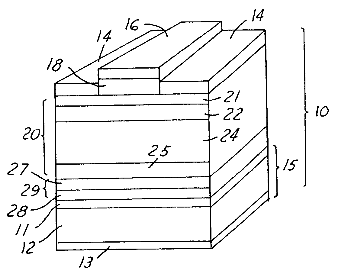
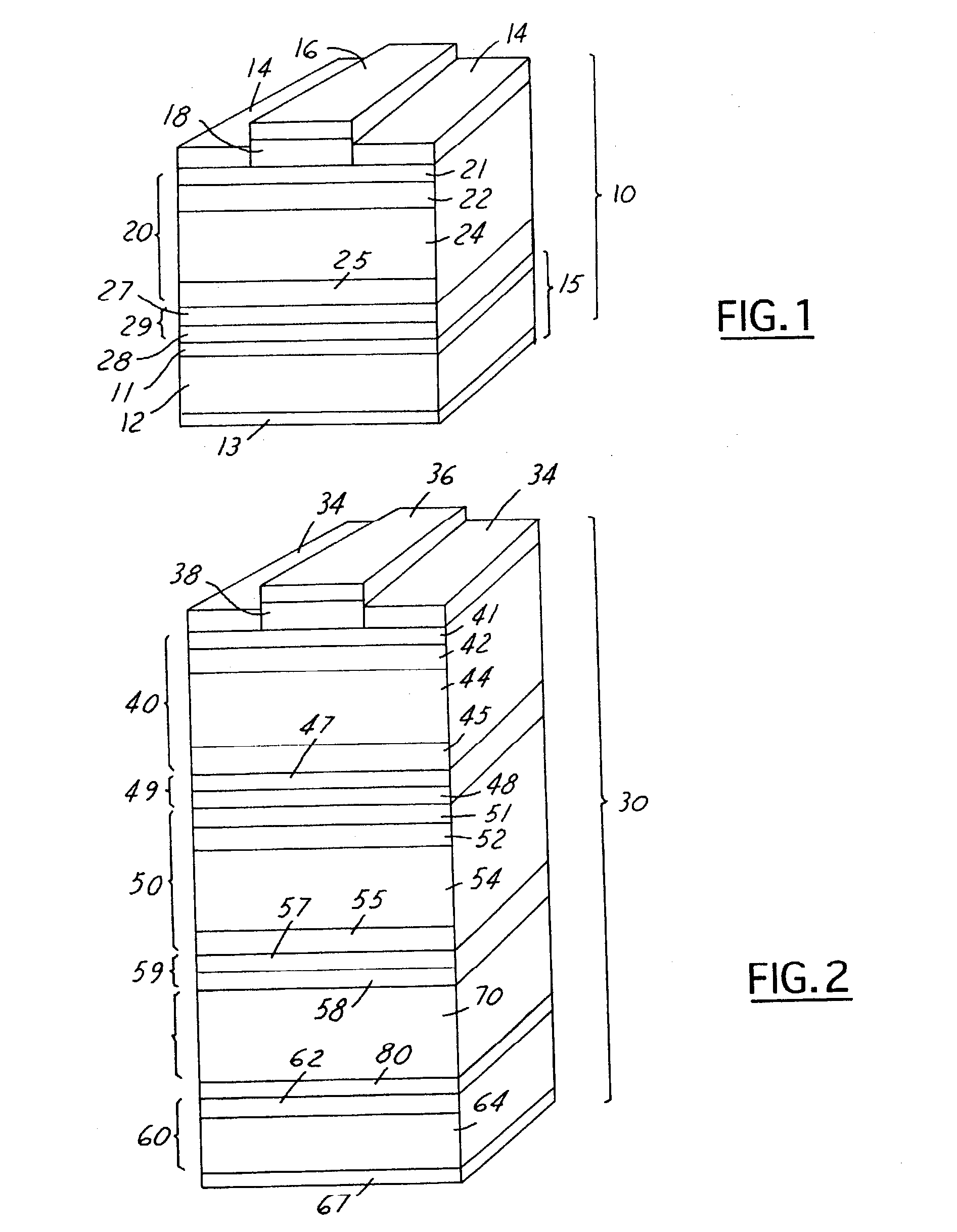
[0015]Single-Junction Photovoltaic Cells

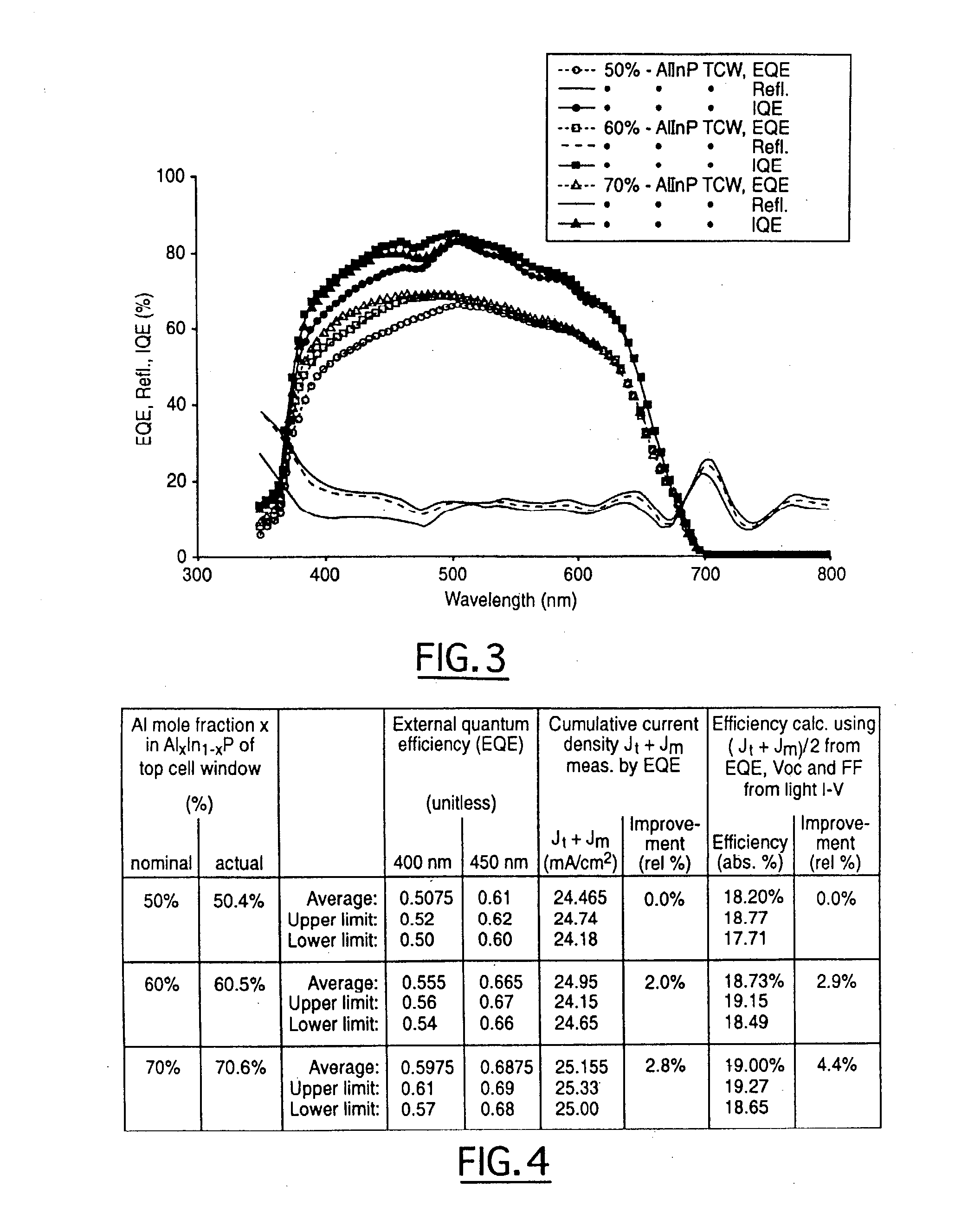
[0016]It is understood that the term “lattice mismatched” refers to the intentional mismatching of material lattice constants between layers of the photovoltaic devices described herein. The term “lattice mismatched,” as one of ordinary skill appreciates, is substantially different than “lattice matched” or “nearly lattice matched.” Also, the term “material lattice constant” refers to the lattice constant of the material in a free-standing layer (i.e. when the material is “relaxed” or “fully relaxed”). In addition, the term “lattice mismatch” of a first layer with respect to a second layer is defined as the difference between the material lattice constant of the first layer and the material lattice constant of the second layer divided by the material lattice constant of the second layer. The term “lattice mismatched,” as one of ordinary skill appreciates, has a greater degree of mismatch and is thus substantially different than “lattice matche...


PUM


Abstract

A photovoltaic cell or other optoelectronic device having a wide-bandgap semiconductor used in the window layer. This wider bandgap is achieved by using a semiconductor composition that is not lattice-matched to the cell layer directly beneath it and/or to the growth substrate. The wider bandgap of the window layer increases the transmission of short wavelength light into the emitter and base layers of the photovoltaic cell. This in turn increases the current generation in the photovoltaic cell. Additionally, the wider bandgap of the lattice mismatched window layer inhibits minority carrier injection and recombination in the window layer.

Description

RELATED APPLICATION[0001]This is a Continuation-In-Part of U.S. patent application Ser. No. 09 / 976,508, filed on Oct. 12, 2001 now abandoned.STATEMENT REGARDING FEDERALLY SPONSORED RESEARCH[0002]This invention was made with Government support under Contract No. F29601-98-2-0207 awarded by the United States Air Force. The Government has certain rights in this invention.TECHNICAL FIELD[0003]The present invention generally relates to semiconductor materials and wide-bandgap, lattice-mismatched layers for optoelectronic devices, and, more particularly, to wide bandgap, lattice-mismatched window layers for solar energy conversion and other photovoltaic devices.BACKGROUND ART[0004]The interest in photovoltaic (“PV”) cells in both terrestrial and non-terrestrial applications continues as concerns over pollution and limited resources continue. Irrespective of the application, and as with any energy generation system, efforts have been ongoing to increase the output and / or increase the effic...

Claims


Application Information

Patent Timeline
IPC IPC(8): H01L31/04H01L21/02H01L31/00H01L31/0216H01L31/0328H01L31/0336H01L31/068H01L31/072H01L31/075H01L31/109
CPCH01L31/02168H01L31/0687H01L31/0725H01L31/076Y02E10/544Y02E10/548H01L31/03046H01L31/03048H01L31/1852Y02E10/547
Inventor KING, RICHARD ROLANDCOLTER, PETER C.ERMER, JAMES H.HADDAD, MORANKARAM, NASSER H.
Owner THE BOEING CO
Why Eureka
Try Eureka