Solar cell and method for manufacturing such a solar cell

a solar cell and manufacturing method technology, applied in the field of solar cells, can solve the problems of reducing the yield of the manufacturing process, adversely affecting the efficiency of the solar cell, and contaminating the front side of the substrate, so as to reduce the creation of defects, improve surface passivation, and reduce the effect of thermal budg

Active Publication Date: 2012-07-19
NEDERLANDSE ORG VOOR TOEGEPAST-NATUURWETENSCHAPPELIJK ONDERZOEK (TNO)
View PDF2 Cites 19 Cited by
  • Summary
  • Abstract
  • Description
  • Claims
  • Application Information

AI Technical Summary

Benefits of technology

[0016]McIntosh et al. (K. R. McIntosh and L. P. Johnson, J. Appl. Phys. 105, 124520-1 (2009) have investigated and reported the benefit of rounding of random pyramid texture of silicon wafers for surface passivation with thermally grown silicon oxide. They find a benefit of rounding for the passivation quality of thick thermal oxide layers (100 nm thick oxide, grown at 1100° C.). The reason is that rounding reduces the creation of defects caused by the volume expansion during the growth of silicon oxide from silicon. However, growth of such thermal oxide layers may require a high thermal budget, which is unfavorable for wafer quality, yield, and production cost.
[0017]It is an object of the present invention to provide a method for manufacturing the solar cell with p- or n-type base, which overcomes or reduces the disadvantages as mentioned above.
[0018]This invention provides a structure and a method for improved surface passivation on textured wafers with diffused emitter and / or diffused BSF and / or diffused FSF.

Problems solved by technology

The screen printing method to form the BSF layer on the back side may cause contamination of the front side of the substrate by parasitic diffusion or spill over of the dopant source to the front side.
Parasitic diffusion of the dopant on the front side results in a non-uniform dopant concentration profile for the emitter layer which will adversely affect the efficiency of the solar cell.
Furthermore, screen printing reduces the yield of the manufacturing process due to a relatively high chance of breakage of substrates.
Also, for n-type BSF layers that use phosphorus as n-type dopant, a one-sided diffusion results in a less efficient gettering of impurities from the substrate.

Method used


Image

  • Solar cell and method for manufacturing such a solar cell
  • Solar cell and method for manufacturing such a solar cell
  • Solar cell and method for manufacturing such a solar cell

Examples


examples

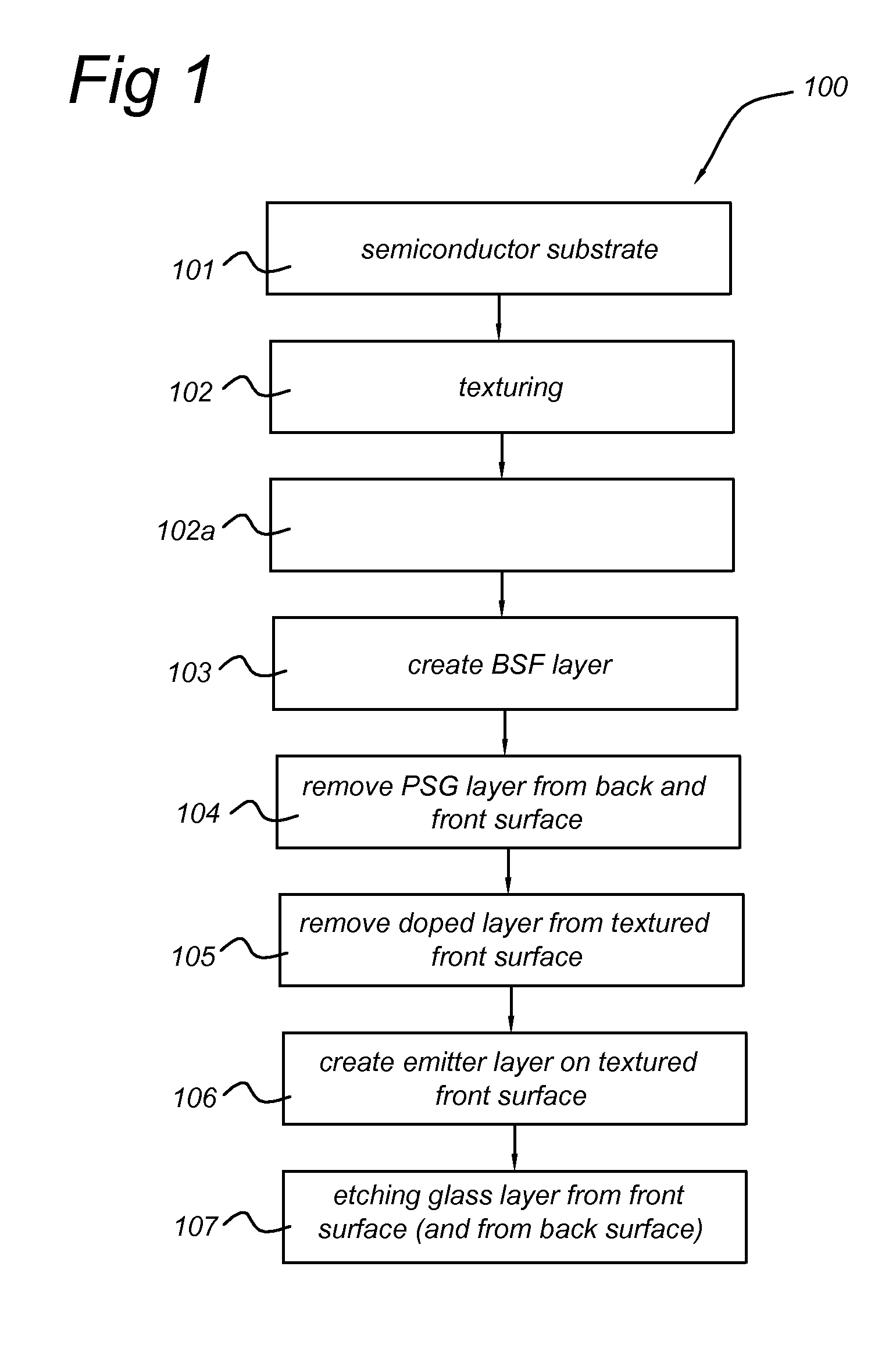
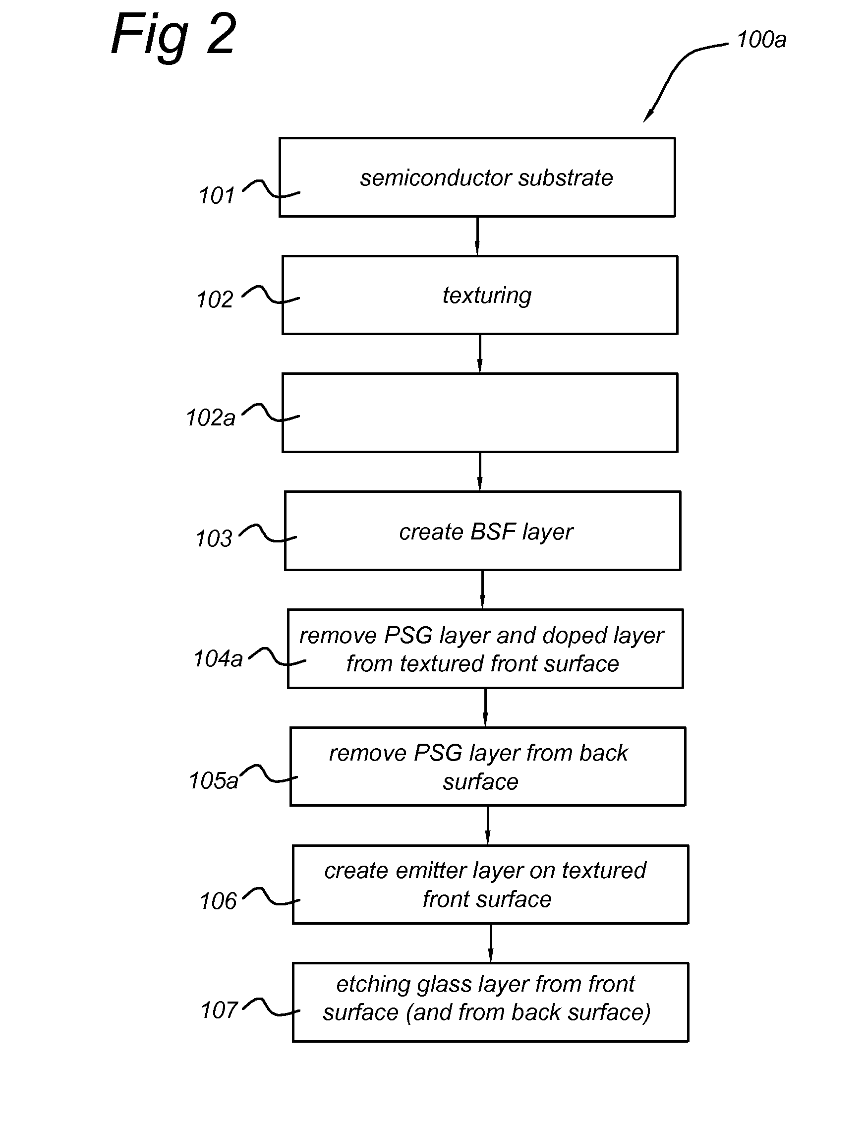
[0213]In an experiment, cells were compared from 3 groups of wafers with the following variation of processing: i) no step 102a, ii) step 102a with a partial smoothening resulting in a wafer thickness reduction >0.1 micron but <1 micron on average, and iii) processed with the same partial smoothening as ii), repeated 3 times total.

[0214]Both groups ii) and iii) showed an increase of 5 mV of the average open circuit voltage, with a statistical uncertainty (95% confidence interval) of 1 mV. The average short circuit current increased by 0.5% with a statistical uncertainty of 0.1%. This clearly proves that the rear surface passivation is improved by the partial smoothening.

no partialonce partialthree times partialsmootheningsmootheningsmootheningVocUo (referenceUo + 5 mV ± 0.5 mVUo + 5 mV ± 0.5 mVvalue)IscIo (referenceIo * (1.005 ± 0.0005)Io * (1.005 ± 0.0005)value)

[0215]In agreement with this, the external quantum efficiency measured with light incident on the rear surface of the cell...


PUM


Abstract

A method for manufacturing a solar cell from a semiconductor substrate (1) of a first conductivity type, the semiconductor substrate having a front surface (2) and a back surface (3). The method includes in a sequence: texturing (102) the front surface to create a textured front surface (2a); creating (103) by diffusion of a dopant of the first conductivity type a first conductivity-type doped layer (2c) in the textured front surface and a back surface field layer (4) of the first conductivity type in the back surface; removing (105; 104a) the first conductivity-type doped layer from the textured front surface by an etching process adapted for retaining texture of the textured front surface; creating (106) a layer of a second conductivity type (6) on the textured front surface by diffusion of a dopant of the second conductivity type into the textured front surface.

Description

FIELD OF THE INVENTION[0001]The present invention relates to a solar cell. Also, the present invention relates to a method for manufacturing such a solar cell.BACKGROUND OF THE INVENTION[0002]Such a solar cell relates to a solar cell with p- or n-type base.[0003]The solar cell comprises a semiconductor substrate, e.g. silicon, which is covered on a back side by the p- or n-type back surface field (BSF) layer and on a front side by an emitter layer of a conductivity type opposite to that of the base layer. The front side of the substrate is arranged to be directed towards a light source during use of the solar cell.[0004]In the prior art, the p- or n-type back surface field layer (BSF layer), is for example manufactured by a screen printing process (but also POCl3 face-to-face tube furnace diffusion, spray coating, spin coating, etc. can be used). During the screen printing process, a paste that comprises a p- or n-type element as dopant element is printed one-sidedly on the back sid...

Claims


Application Information

Patent Timeline
Patent Type & Authority Applications(United States)
IPC IPC(8): H01L29/34H01L31/18
CPCH01L31/18H01L31/02363Y02E10/50Y02E10/547Y02E10/548H01L31/068H01L31/02167
Inventor GEERLIGS, LAMBERT JOHANLI, GAOFEIBARTON, PAUL CORNELISNABER, RONALD CORNELIS GERARDSTASSEN, ARNO FERDINANDHU, ZHIYAN
Owner NEDERLANDSE ORG VOOR TOEGEPAST-NATUURWETENSCHAPPELIJK ONDERZOEK (TNO)
Why Eureka
Try Eureka