Multi-port memory based on DRAM core

a multi-port memory and dram core technology, applied in the field of semiconductor memory devices, can solve the problems of large size of memory cells, and large capacity of multi-port memory

Inactive Publication Date: 2006-10-10
SOCIONEXT INC
View PDF21 Cites 41 Cited by
  • Summary
  • Abstract
  • Description
  • Claims
  • Application Information

AI Technical Summary

Benefits of technology

[0021]The invention as described above is provided with the first operation mode in which a refresh operation is performed in response to an instruction from an external port and with the second operation mode in which a refresh operation is performed in response to the internal refresh circuit. Because of this configuration, one of the external ports is allowed to operate as a port for refresh management so as to receive refresh commands at constant internals, or the internal refresh circuit performs refresh operations if this port for refresh management is in a deactivated state. This makes it possible to manage refresh operations in a flexible manner according to system configurations.

Problems solved by technology

As a result, a multi-port memory needs a large capacity.
The SRAM-type multi-port memories, however, have a drawback in that the size of a memory cell is large.
This is because only a destructive read operation is possible in a DRAM cell.
Further, once in a BUSY state, the DRAM-type multi-port memory suffers problems that desired operations cannot be performed, or that processing becomes slow due to a waiting time.

Method used


Image

  • Multi-port memory based on DRAM core
  • Multi-port memory based on DRAM core
  • Multi-port memory based on DRAM core

Examples


first embodiment

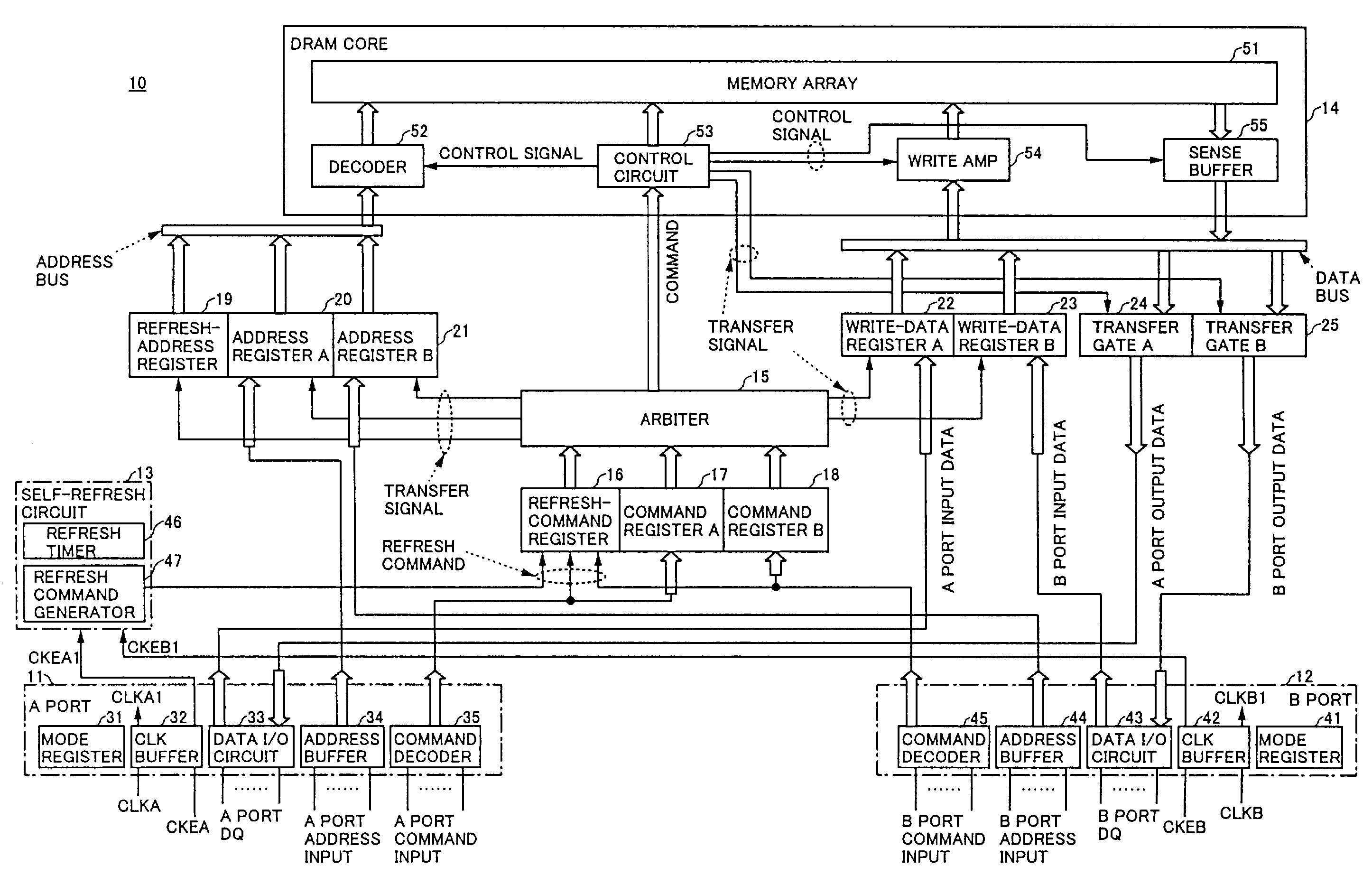
[0183]FIG. 4 is a block diagram showing the multi-port memory according to the present invention. In this example, a configuration is such that two ports, i.e., an A port and a B port, are provided.

[0184]A multi-port memory 10 of FIG. 4 includes an A port 11, a B port 12, a self-refresh circuit 13, a DRAM core 14, an arbiter 15, a refresh-command register 16, a command register A 17, a command register B 18, a refresh-address register 19, an address register A 20, an address register B 21, a write-data register A 22, a write-data register B 23, a transfer gate A 24, and a transfer gate B 25.

[0185]The A port 11 includes a mode register 31, a CLK buffer 32, a data I / O circuit 33, an address buffer 34, and a command decoder 35. Further, the B port 12 includes a mode register 41, a CLK buffer 42, a data I / O circuit 43, an address buffer 44, and a command decoder 45. At the A port 11 and the B port 12, access to / from an external bus is established independently in synchronization with re...

second embodiment

[0248]FIG. 23 is a drawing for explaining the present invention.

[0249]In general, memory is extended according to usage thereof. The same applies in the case of a multi-port memory, and there may be a case in which a plurality of multi-port memories is provided for the purpose of expanding memory space.

[0250]A multi-port memory includes an arbiter, and detects which one of the commands are earlier in entering the respective ports, followed by executing commands in the detected order. Even when commands are input at almost the same timing-to the respective ports, an order is determined for successive execution of the commands. In an example shown in FIG. 23, a plurality of multi-port memories 200-1 through 200-n are provided, and the same commands are supplied to the multi-port memories 200-1 through 200-n from an A port controller 201 and a B port controller 202. The relative timing of command arrival at each multi-port memory may slightly differ because of different lengths of sign...

third embodiment

[0607]In the following, operations of the multi-port memory M will be described.

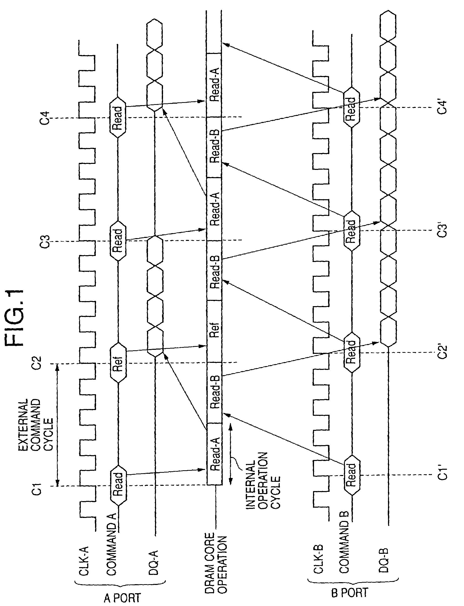
[0608]FIG. 127 shows the way a read operation is performed when the input / output ports PORT-A and PORT-B receive active commands ACT and the same row address signals RA. The phase of the clock signal CLKA is slightly ahead of the phase of the clock signal CLKB. Namely, inputting of an active command ACT to the input / output port PORT-A is slightly earlier than entering of an active command ACT in the input / output port PORT-B.

[0609]With respect to the input / output port PORT-A, a read operation READ is performed in response to the active command ACT (FIG. 127-(a)). Data read from memory cells are stored in the data register 5046a (or 5046b). With respect to the input / output port PORT-B, then, a read operation READ is performed in response to the active command ACT (FIG. 127-(b)). The read operation READB with respect to the input / output port PORT-B is performed after the completion of the read operation RE...


PUM


Abstract

A semiconductor memory device includes a plurality of N external ports, each of which receives commands, and an internal circuit which performs at least N access operations during a minimum interval of the commands that are input into one of the external ports.

Description

[0001]This is a continuation-in-part application of U.S. patent application Ser. No. 09 / 968,516, filed Oct. 2, 2001.BACKGROUND OF THE INVENTION[0002]1. Field of the Invention[0003]The present invention generally relates to semiconductor memory devices, and particularly relates to a semiconductor memory device equipped with a plurality of ports.[0004]2. Description of the Related Art[0005]Multi-port memories, which are semiconductor memory devices equipped with a plurality of ports, can be classified into various types. When the term “multi-port memory” is used hereinafter, it refers to a memory that is provided with a plurality of ports, and that allows access to be independently made from any one of the ports to a common memory array. Such a memory may have an A port and a B port, and allows a read / write operation to be conducted with respect to the common memory array independently from a CPU linked to the A port and from a CPU linked to the B port.[0006]A multi-port memory is equ...

Claims


Application Information

Patent Timeline
Patent Type & Authority Patents(United States)
IPC IPC(8): G06F12/00G11C7/22G11C8/16G11C8/18G11C11/409
CPCG06F13/1605G11C7/1039G11C7/1078G11C7/22G11C8/16G11C8/18G11C11/406G11C11/40603G11C11/40615G11C11/409G11C11/4093G11C11/24G11C7/1075G11C2207/107G11C2207/108
Inventor MATSUZAKI, YASUROUSUZUKI, TAKAAKIYAMAZAKI, MASAFUMIKAWASAKI, KENICHIKAMATA, SHINNOSUKESATO, AYAKOMATSUMIYA, MASATO
Owner SOCIONEXT INC
Why Eureka
Try Eureka