

Vertical probe card and air cooled probe head system
a probe head and vertical probe technology, applied in semiconductor/solid-state device testing/measurement, fault location by increasing destruction at fault, etc., can solve the problems of conventional techniques, and neither heat transfer channel prevents the use of conventional polyimide or other similar printed circuit board materials
- Summary
- Abstract
- Description
- Claims
- Application Information
AI Technical Summary
Benefits of technology
Problems solved by technology
Method used
Image

Examples
Embodiment Construction
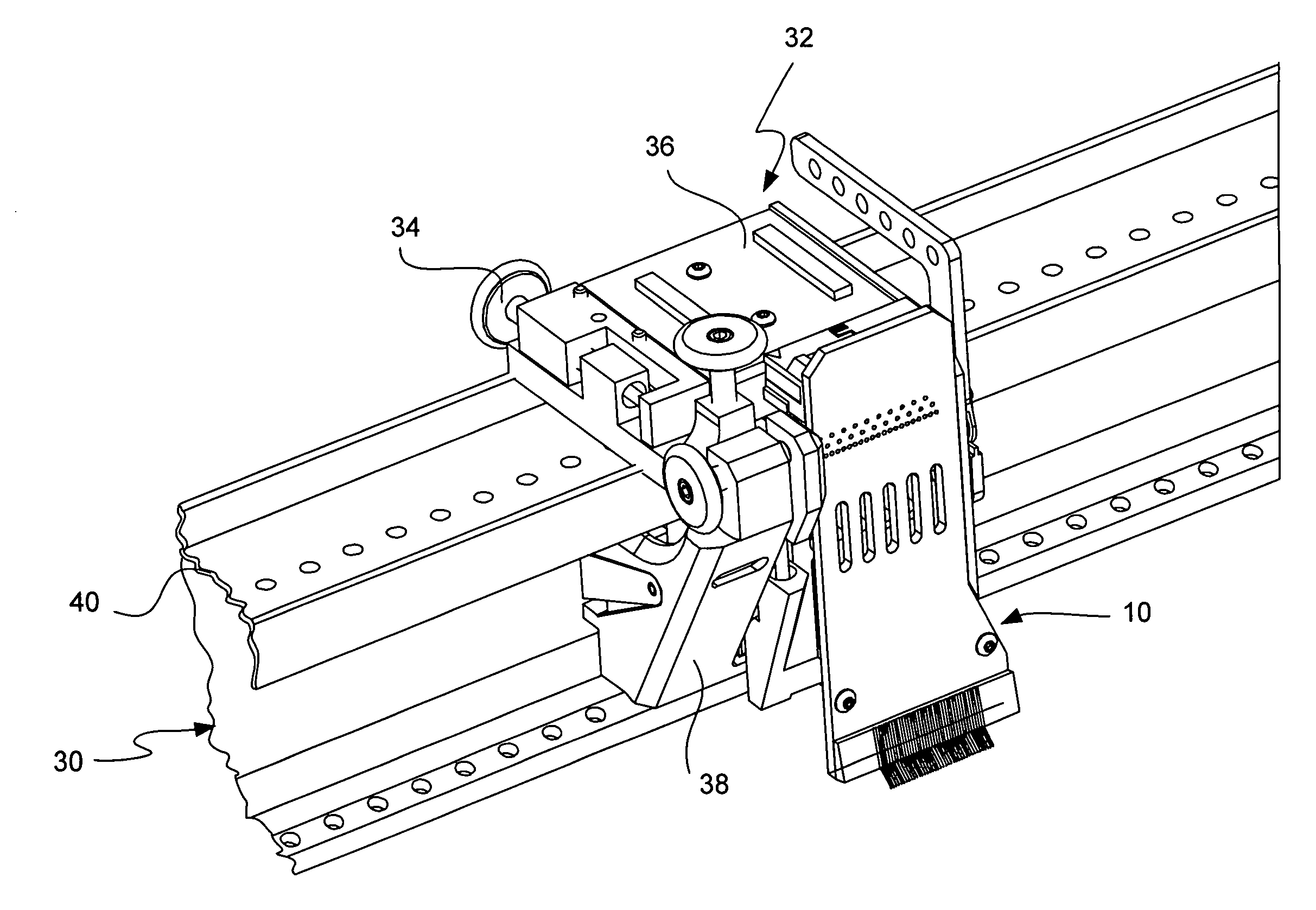
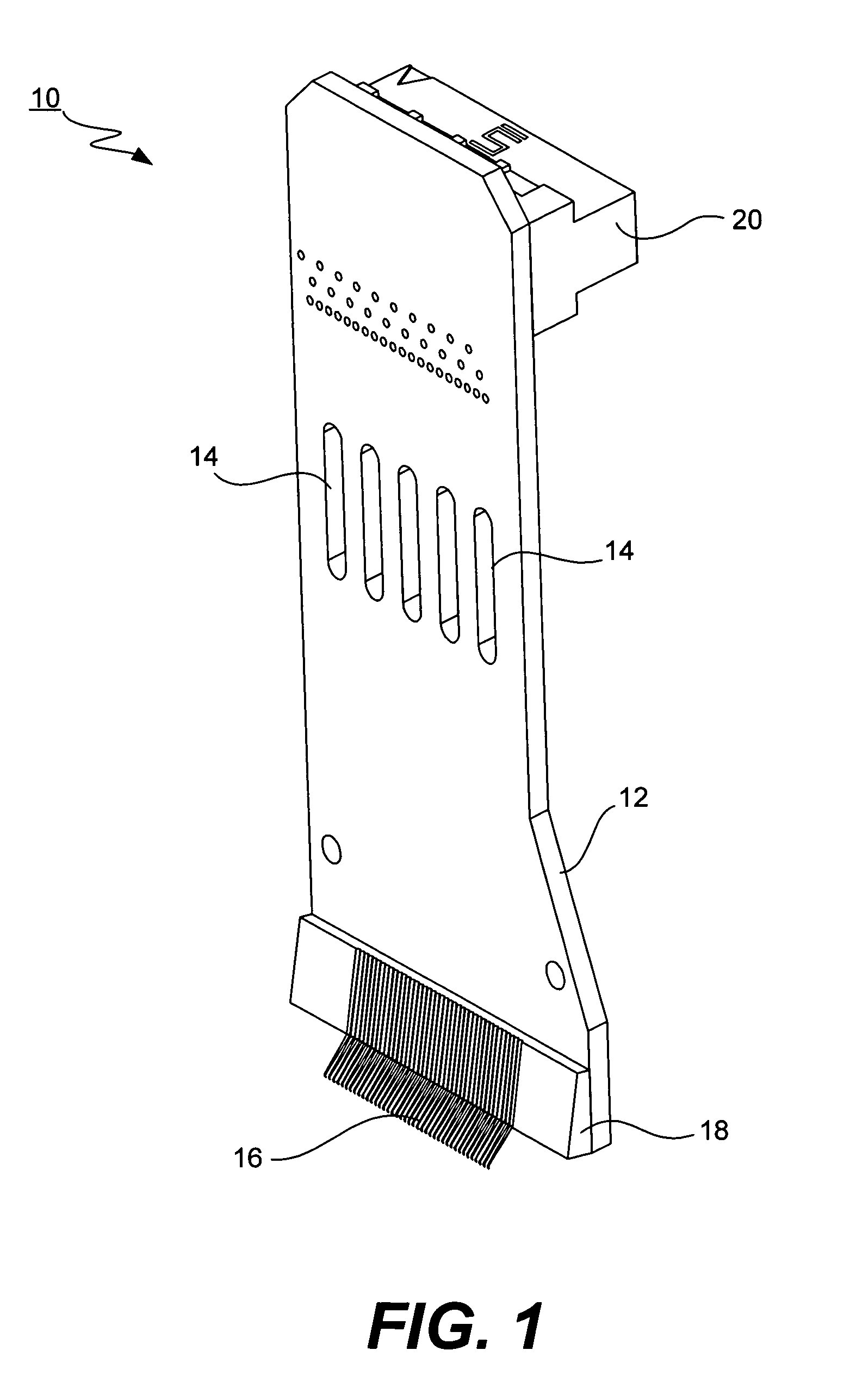
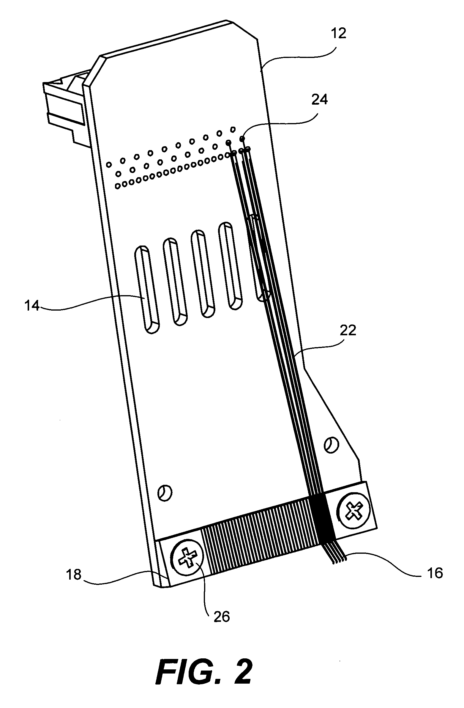
[0020]FIG. 1 is a perspective view of a probe card 10 in accordance with one embodiment of the invention and includes a printed circuit board 12 with a plurality of slots 14 therethrough for facilitating the flow of cool air. At one end of board 12 is a tip assembly including a plurality of metal probe tips 16 in a ceramic support 18 and on an opposing end of printed circuit board 12 is an electrical connector and fastener 20 which is used for physically supporting the probe card in a test system and connects the tips 16 to a flexible (flex) cable.
[0021]FIG. 2 is a plan view further illustrating printed circuit board 12 and metal traces 22 which electrically interconnect the probe tips 16 to electrical contacts 24 on the opposing end of board 12. The electrically conductive pattern of metal traces or discrete wires 22 interconnect individual probe tips to one of the contacts 24. As illustrated, ceramic support 18 with probe tips 16 supported therein is attached to board 12 by means ...
PUM
 Abstract
Description
Claims
Application Information