Method of manufacturing electronic device including aligning first substrate, second substrate and mask, and transferring object from first substrate to second substrate, including irradiating object on first substrate with light through mask

a manufacturing method and electronic device technology, applied in the direction of solid-state devices, feeding apparatus, printed circuit assembling, etc., can solve the problems of increasing equipment cost, difficult to ensure the degree of positioning accuracy when adhering to the substrates, and difficulty in performing inter-substrat alignment with a high degree of accuracy, etc., to facilitate the manufacture of electronic devices. , the effect of large-scale electric optical devices

Active Publication Date: 2006-10-31
SAMSUNG ELECTRONICS CO LTD
View PDF5 Cites 114 Cited by
  • Summary
  • Abstract
  • Description
  • Claims
  • Application Information

AI Technical Summary

Benefits of technology

[0029]Preferably, a piece of piezoelectric element is used as both the pressure sensor and the minutely elastic object. Accordingly, downsizing can easily be realized.
[0030]Preferably, the object to be transferred includes a thin film element or a thin film circuit. Accordingly, transfer in single thin film elements or transfer in single film circuits are achieved, whereby manufacture of the electronic device is facilitated. In particular, manufacture of large sized electric optical devices (Liquid Crystal Displays, organic EL displays, and so on) is facilitated.

Problems solved by technology

In addition, in inter-substrate transfer, when the substrate is formed of a flexible material, such as an organic film substrate, or when an original substrate and a destination substrate are formed of different materials, it is difficult to ensure the degree of positioning accuracy when adhering them together.
In other words, the organic film substrate is liable to undulate or warp, and thus it is difficult to perform inter-substrate alignment with a high degree of accuracy.
This may cause increase in cost of equipment.

Method used


Image

  • Method of manufacturing electronic device including aligning first substrate, second substrate and mask, and transferring object from first substrate to second substrate, including irradiating object on first substrate with light through mask
  • Method of manufacturing electronic device including aligning first substrate, second substrate and mask, and transferring object from first substrate to second substrate, including irradiating object on first substrate with light through mask
  • Method of manufacturing electronic device including aligning first substrate, second substrate and mask, and transferring object from first substrate to second substrate, including irradiating object on first substrate with light through mask

Examples


Embodiment Construction

[0069]An exemplary embodiment of the present invention is discussed below with reference to the drawings.

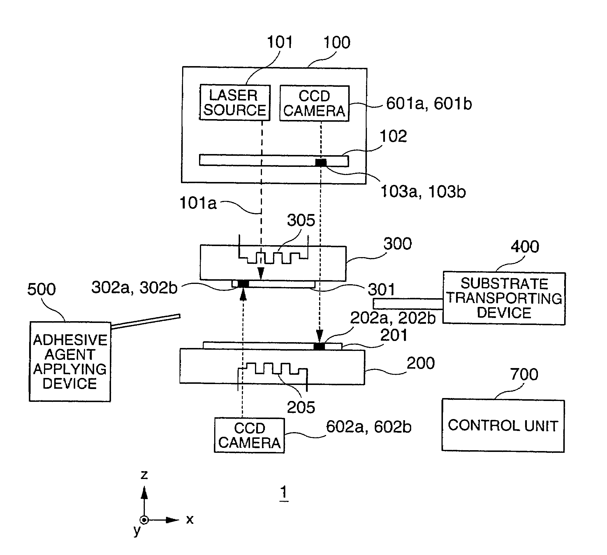
[0070]FIG. 1 is a schematic illustrating an apparatus for manufacturing electronic devices in which the electronic device is assembled according to the inter-substrate transfer technology according to the present invention.

[0071]As shown in the same drawing, a manufacturing apparatus 1 generally includes an optical unit 100 to emit a laser for transfer, an A stage 200 to place a destination substrate, a B stage 300 to place an original substrate, a substrate transporting unit 400 to transport the substrate to each stage, an adhesive agent applying unit 500 to partially apply an adhesive agent onto any one of substrates, CCD cameras 601a, 601b, 602a, and 602b to detect a mark to adjust alignment of the original substrate and the destination substrate, and a control unit 700 including a computer system to control the manufacturing process.

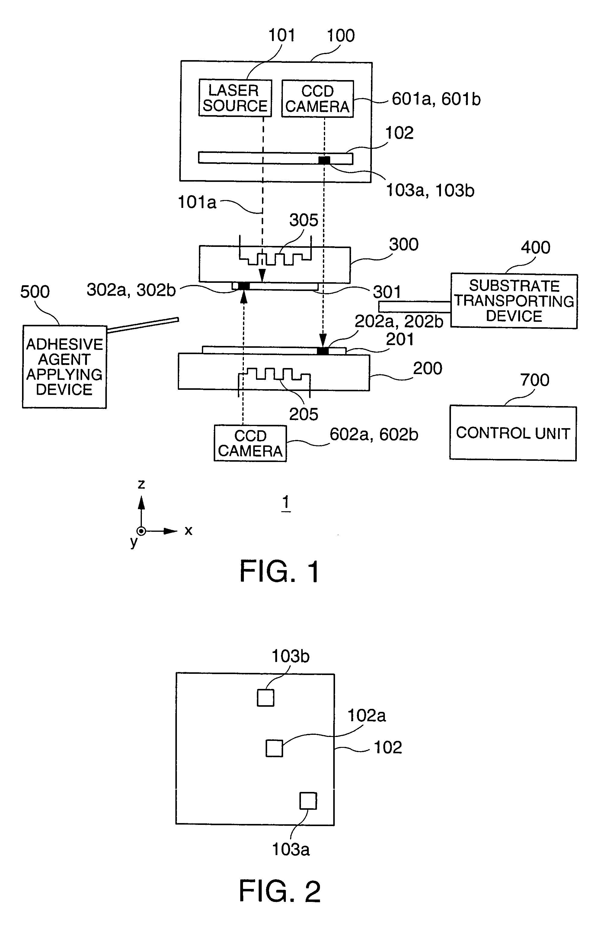
[0072]The optical unit 100 is secured to a ...


PUM

PropertyMeasurementUnit
flexibleaaaaaaaaaa
transmissionaaaaaaaaaa
sizeaaaaaaaaaa

Abstract

A method of manufacturing an electronic device includes providing a mask substrate, a first substrate on which an object to be transferred is formed, and a second substrate to which the object is to be transferred, adjusting positions of the mask substrate, the first substrate and the second substrate so that an alignment mark formed on one of the substrates (a reference substrate) and alignment marks formed on other two of the substrates are aligned with each other, and transferring the object to be transferred from the first substrate to the second substrate, the transferring step including irradiating the object to be transferred from the first substrate with light transmitted through the mask substrate.

Description

BACKGROUND OF THE INVENTION[0001]1. Field of Invention[0002]The present invention relates to a manufacturing apparatus and a manufacturing method of manufacturing electronic devices using inter-substrate transferring technology to transfer an electronic device from one substrate to another substrate.[0003]2. Description of Related Art[0004]The related art includes technology of transferring an electronic device from an original substrate to another substrate. For example, a TFT-LCD (Liquid Crystal Display) manufactured on a quartz substrate in a low temperature polysilicon TFT (Thin Film Transistor) process is transferred onto a plastic substrate so as to facilitate assembling of the LCD on the plastic substrate in the form of a film, which is low in capacity for resisting heat. For example, Japanese Unexamined Patent Application Publication No. 11-142878 discloses a method of forming a display panel with transistor array, in which the TFT element is selectively transferred.[0005]In...

Claims


Application Information

Patent Timeline
Patent Type & Authority Patents(United States)
IPC IPC(8): H05K3/30G02F1/13B23K26/02B23K26/067B23K101/36G02F1/1368G09F9/00H01L21/02H01L21/98H01L27/12H01L51/00H01L51/40H01L51/50H05B33/10
CPCB23K26/0608B23K26/067H01L25/50H01L51/0013B23K26/0656Y10T29/53178H01L51/0009H01L2924/0002Y10T29/49131Y10T29/53174Y10T29/53196Y10T29/53187Y10T29/5313Y10T29/49144Y10T29/49126Y10T29/4913Y10T29/53091Y10T29/53087Y10T29/53052H01L2924/00B23K26/066H10K71/162H10K71/18H01L21/027
Inventor KASUGA, MASASHIKAMAKURA, TOMOYUKIMIYAZAWA, WAKAOTSUCHIHASHI, FUKUMI
Owner SAMSUNG ELECTRONICS CO LTD
Why Eureka
Try Eureka