Process for producing a multi-layer printed wiring board

a multi-layer printed, wiring board technology, applied in the direction of printed circuit assembling, circuit masks, metallic pattern materials, etc., can solve the problems of high accuracy, difficult control, and current method of manufacture that cannot guarantee the accurate positioning of laser irradiation, and achieve the effect of reducing the reflectivity

Inactive Publication Date: 2006-10-31
IBIDEN CO LTD
View PDF19 Cites 15 Cited by
  • Summary
  • Abstract
  • Description
  • Claims
  • Application Information

AI Technical Summary

Benefits of technology

[0091]In this way it is possible to form via holes at adequate positions even though the accuracy of position for laser irradiation is not high, because the accuracy of the position of via holes depends solely on the accuracy of the position of the openings in the metal film (or conformal mask).
[0128]The deposited metal film and the electrolessly-plated film covering it should preferably be thinner than 2 μm. Such a thin film is easily removed by etching when conductor circuits and via holes are formed by removing unnecessary parts of the metal film and electrolessly plated layer. Therefore, the electrolytically plated layer used to form conductor circuits and via holes are not damaged by the etching process. Thus it is possible to create wiring with a fine pitch and via holes with an extremely small diameter.

Problems solved by technology

Unfortunately, it has been difficult to control, with high accuracy, the position of laser irradiation for via hole drilling in mass production.
However, the current method of manufacture can not guarantee accurate positioning of laser irradiation.
Improvement in positioning accuracy is offset by a necessary decrease in head driving speed, which in turn lowers productivity.

Method used


Image

  • Process for producing a multi-layer printed wiring board
  • Process for producing a multi-layer printed wiring board
  • Process for producing a multi-layer printed wiring board

Examples


Embodiment Construction

[0143]The embodiments of the present invention will be described with reference to the drawings.

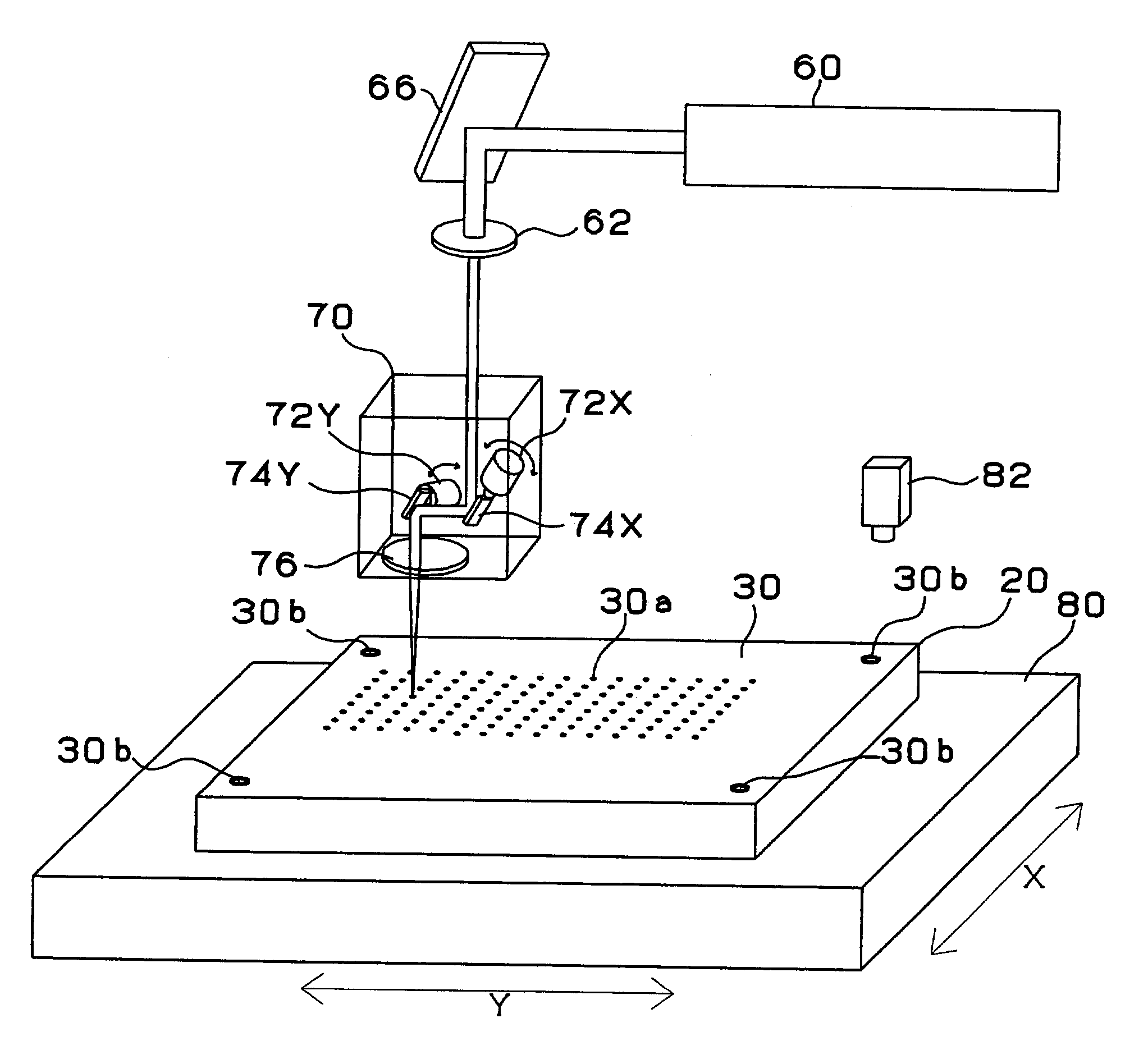
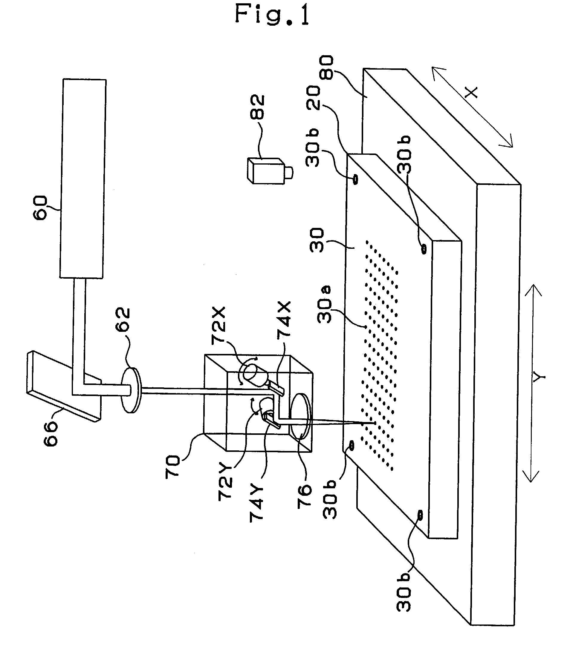
[0144]The first embodiment of the present invention employs an apparatus as shown in FIG. 1 for production of a multi-layer printed wiring board.

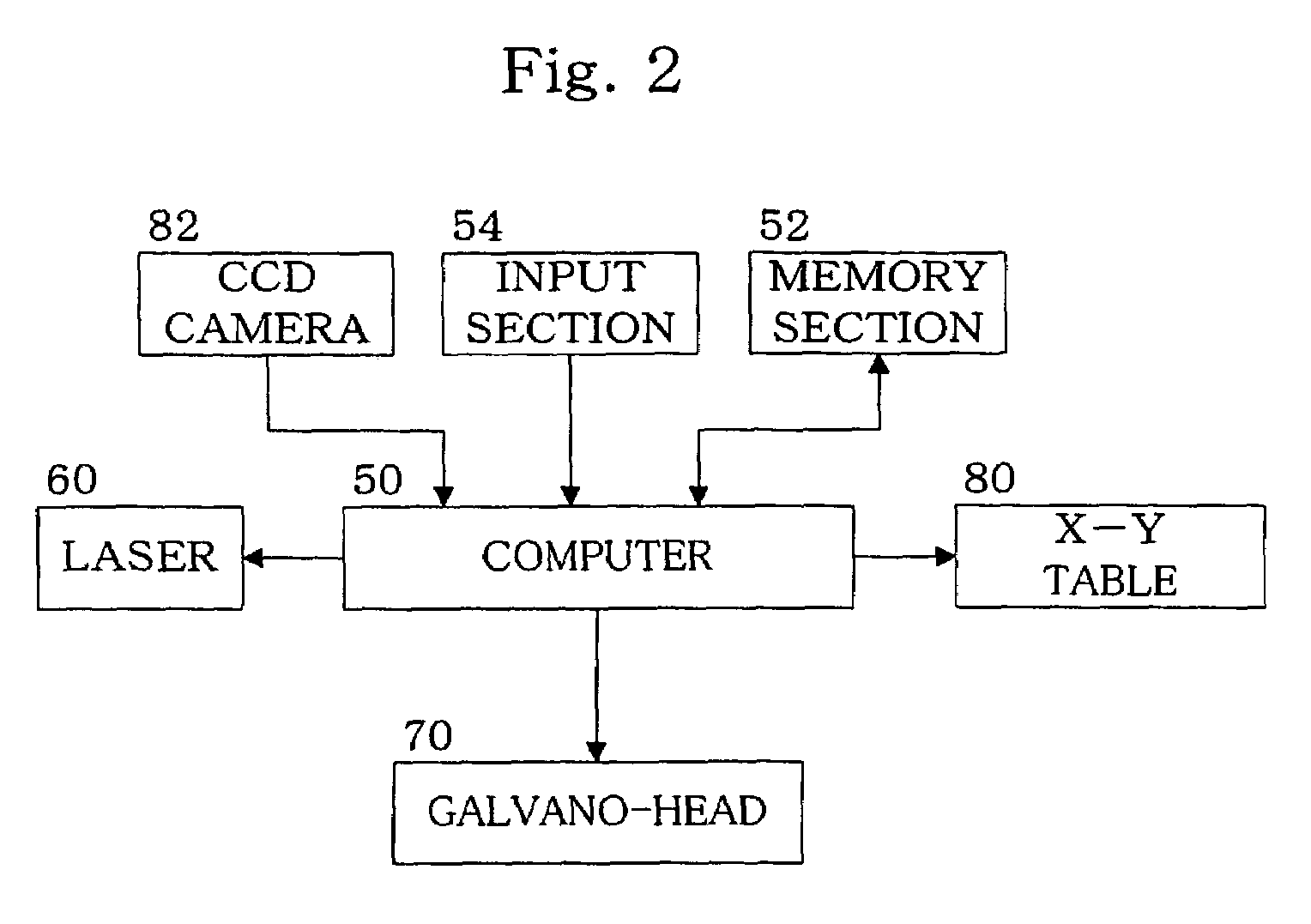
[0145]In this embodiment, a CO2 laser emitter 60 generates a laser beam. The laser beam is reflected by a mirror 66 and transmitted to a galvano head 70 through a transfer mask 62 for sharp focusing on the board.

[0146]The galvano-head (scanning head) 70 is composed of a set of galvano-mirrors including; a galvano-mirror 74X for scanning the laser beam in an X direction and a galvano-mirror 74Y for scanning the beam in a Y direction. Control motors 72X, 72Y drive these mirrors 74X, 74Y. The motors 72X, 72Y adjust the angles of the mirrors 74X,74Y depending on the control command from the computer (to be explained later), and also transmit the detection signal from the built-in encoder to the computer side.

[0147]The scan area of the galvano-mirror ...


PUM

PropertyMeasurementUnit
diameteraaaaaaaaaa
particle diameteraaaaaaaaaa

Abstract

A board 20 is provided with a Cu film 30 as a conformal mask, in which are formed a register mark 30b and an opening 3a through which a via hole is formed. A camera senses this register mark 30b so that the position of the board 30 is determined. A laser beam is directed to the approximate position of the opening 30a, so that the opening 26a through which the via hole is drilled is formed. The accuracy of the position of the opening of the via hole depends on the accuracy of the position of the opening 30a in the Cu film 30 as the conformal mask. Therefore, the via hole can be formed at an adequate position despite the low accuracy of the position for laser irradiation.

Description

[0001]The present application is a division of application Ser. No. 09 / 581,298, filed on Jun. 12, 2000, now U.S. Pat. No. 6,609,297, which is a 371 of International Application No. PCT / JP98 / 05398, filed Nov. 30, 1998, which claims priority to Japanese Application No. H9-362132, filed on Dec. 11, 1997.TECHNICAL FIELD[0002]The present invention relates to a process for producing a multi-layer printed wiring board, said process permitting mass production of a multi-layer printed wiring board with small-diameter via holes. Increased productivity is made possible, by driving the galvano head at a higher speed.BACKGROUND ART[0003]A build-up multilayer wiring board alternately has interlayer resin insulators and conductive circuit layers, provides holes to the interlayer resin insulator layers, and then electrically connects the upper layers and lower layers by forming conductive films on the surface of the walls of these holes.[0004]A hole (via hole) in the interlayer resin insulating lay...

Claims


Application Information

Patent Timeline
Patent Type & Authority Patents(United States)
IPC IPC(8): H01K3/10H05K1/02H05K3/00H05K3/46
CPCH05K3/0035H05K3/4652H05K3/4655H05K3/4679H05K3/0008H05K1/0269Y10S430/146H05K3/0082H05K3/421H05K2201/09781H05K2201/09918H05K2203/0554Y10T29/49165Y10T29/49082Y10T29/49155Y10T29/49085Y10T29/49004Y10T29/49126Y10T29/49117Y10T29/49156
Inventor HIRAMATSU, YASUJIASAI, MOTOOHIROSE, NAOHIROKARIYA, TAKASHI
Owner IBIDEN CO LTD
Why Eureka
Try Eureka