Semiconductor integrated circuit and methods for protecting the circuit from reverse engineering

a technology of integrated circuits and semiconductors, applied in the direction of conveying record carriers, pulse techniques, instruments, etc., can solve the problems that conventional methods for preventing reverse engineering require additional circuitry or additional processing, and achieve the effect of being ready to implemen

Inactive Publication Date: 2006-10-31
SAMSUNG ELECTRONICS CO LTD
View PDF5 Cites 22 Cited by
  • Summary
  • Abstract
  • Description
  • Claims
  • Application Information

AI Technical Summary

Benefits of technology

[0006]Exemplary embodiments of the present invention include a semiconductor integrated circuit that comprises a reverse engineering protection part and method, which can be readily implemented without the need for additional circuitry or additional processing.

Problems solved by technology

However, conventional methods for preventing reverse engineering require additional circuitry or additional processing.

Method used


Image

  • Semiconductor integrated circuit and methods for protecting the circuit from reverse engineering
  • Semiconductor integrated circuit and methods for protecting the circuit from reverse engineering
  • Semiconductor integrated circuit and methods for protecting the circuit from reverse engineering

Examples


Embodiment Construction

[0023]The embodiments of the present invention will now be described in further detail with reference to the accompanying drawings. In the drawings, like reference numerals are used to refer to like elements throughout.

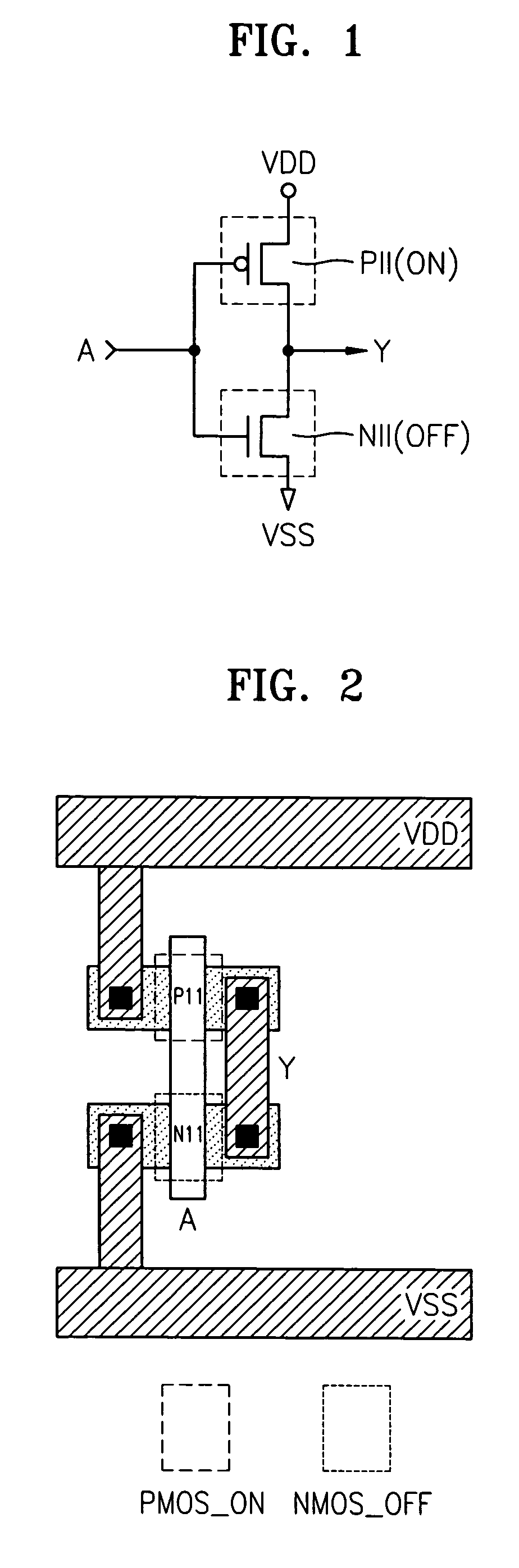
[0024]FIG. 1 is a circuit diagram of an inverter including a reverse engineering protection part according to an exemplary embodiment of the present invention and FIG. 2 illustrates a top view circuitry design picture of the inverter of FIG. 1, which is obtained after decapsulation of the inverter.

[0025]Referring to FIG. 1, an inverter includes a PMOS transistor P11 and NMOS transistor N11. The PMOS transistor P11 is connected between a supply voltage node having a voltage of VDD and an output terminal Y and has a gate to which an input signal A is applied. The NMOS transistor N11 is connected between the output terminal Y and a voltage VSS or ground and has a gate to which the input signal A is applied.

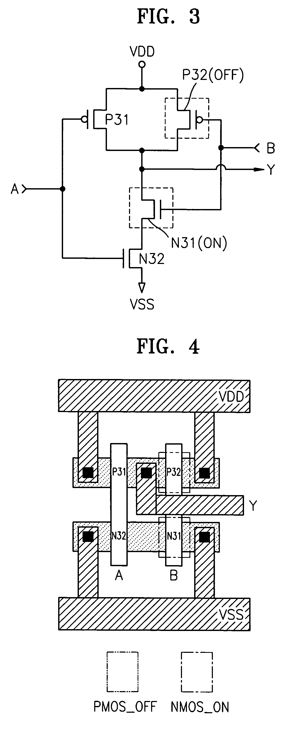
[0026]According to another embodiment of the present invention, o...


PUM


Abstract

A semiconductor integrated circuit having a reverse engineering protection part that can be easily implemented without additional circuitry or process using a method for protecting against reverse engineering of the semiconductor integrated circuit. The semiconductor integrated circuit includes a logic gate and a reverse engineering protection part. The reverse engineering protection part alters the apparent Boolean functions of a logic gate. Further, the reverse engineering protection part includes at least one PMOS transistor and at least one NMOS transistor. The PMOS and NMOS transistors are constructed to remain in a state of constant on or off irrespective of an input signal applied to their gates. The PMOS transistors and the NMOS transistors are included in transistors forming the logic gate. The PMOS transistors and the NMOS transistors that remain in a state of constant on or off are formed by implanting ions into their gate channels or blocking ion implantation into their gate channels during manufacturing.

Description

CROSS REFERENCE TO RELATED APPLICATION[0001]This application claims priority to Korean Patent Application No. 2003-50345, filed on Jul. 22, 2003, in the Korean Intellectual Property Office, the disclosure of which is hereby incorporated by reference.BACKGROUND[0002]1. Technical Field[0003]The present invention relates to a semiconductor integrated circuit, and more particularly, to a semiconductor integrated circuit including a reverse engineering protection part and a method for protecting against reverse engineering of an integrated circuit.[0004]2. Discussion of the Related Art[0005]Semiconductor integrated circuits are often reverse engineered for the purpose of extracting circuits embedded in semiconductor devices. To prevent such reverse engineering, a variety of methods have been suggested. For example, U.S. Pat. No. 6,294,816 discloses a method of using implanted interconnections to replace metal interconnects to connect doped circuit elements. Since such implanted interconn...

Claims


Application Information

Patent Timeline
Patent Type & Authority Patents(United States)
IPC IPC(8): G06K13/00G06F21/75H01L27/10H01L23/58H01L27/02H01L27/092H03K19/00
CPCG06F21/75H01L23/576H01L27/02H01L27/0207H01L2924/0002H01L2924/00H01L27/10
Inventor KIM, JONG-CHEOL
Owner SAMSUNG ELECTRONICS CO LTD
Why Eureka
Try Eureka