Mask etch processing apparatus

a technology of mask etching and processing apparatus, which is applied in the direction of chemical vapor deposition coating, coating, electric discharge tube, etc., can solve the problems of defective photomasks, only selective exposure of the resist layer, and light transmission properties of the substrate, so as to minimize contact and minimize the formation of defects in the substrate

Active Publication Date: 2006-10-31
APPLIED MATERIALS INC
View PDF43 Cites 140 Cited by
  • Summary
  • Abstract
  • Description
  • Claims
  • Application Information

AI Technical Summary

Benefits of technology

[0011]The present invention generally provides a substrate support member to minimize defect formation in a substrate during processing and handling of substrates in a plasma etch chamber. In one aspect, an apparatus is provided for supporting a substrate on a pedestal or cathode in a processing chamber to minimize contact between the substrate and the chamber components during processing.

Problems solved by technology

However, the photoresist layer is only selectively exposed.
These defects can alter the light transmission properties of the substrates and result in defective photomasks.

Method used


Image

  • Mask etch processing apparatus
  • Mask etch processing apparatus
  • Mask etch processing apparatus

Examples


Embodiment Construction

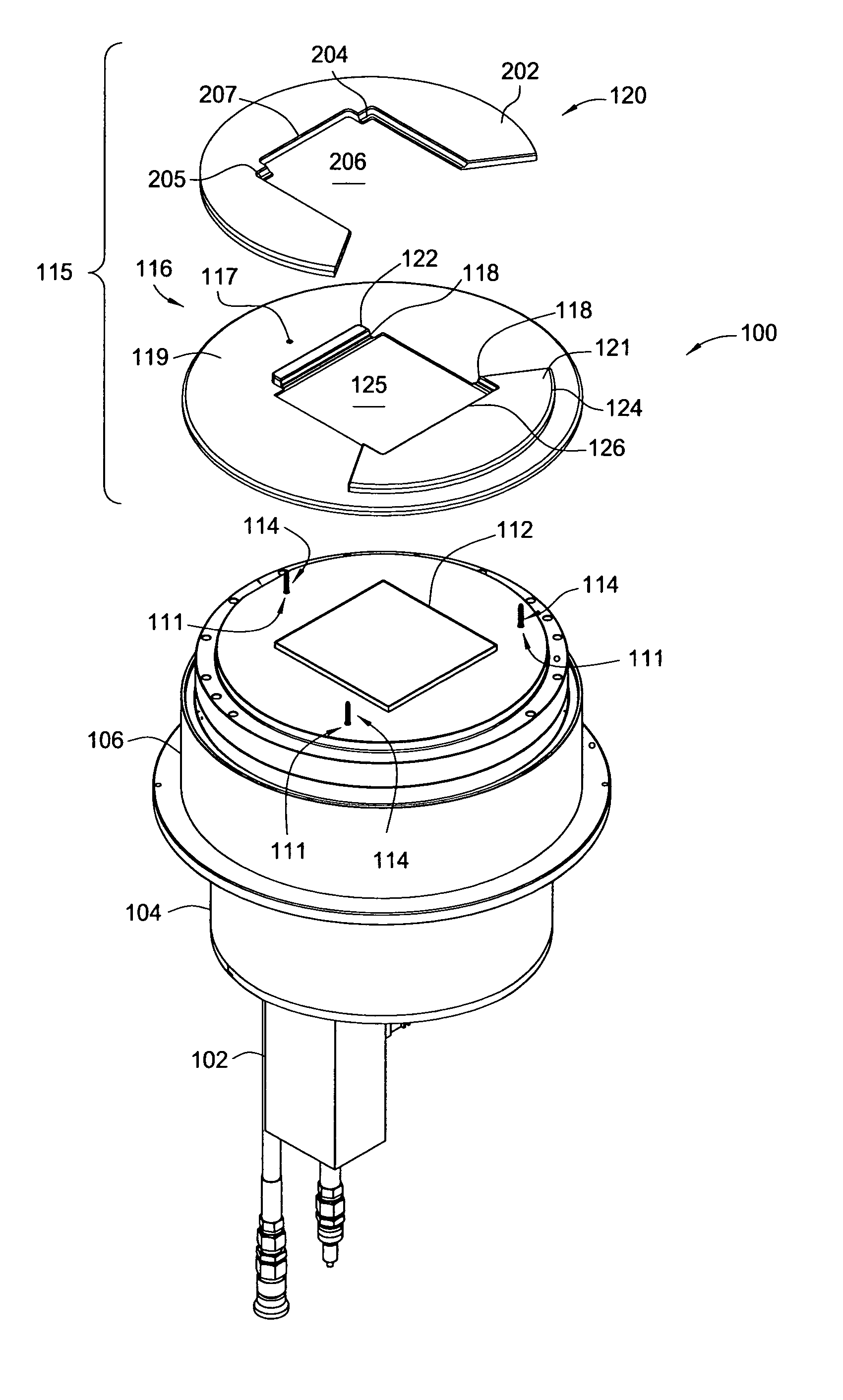
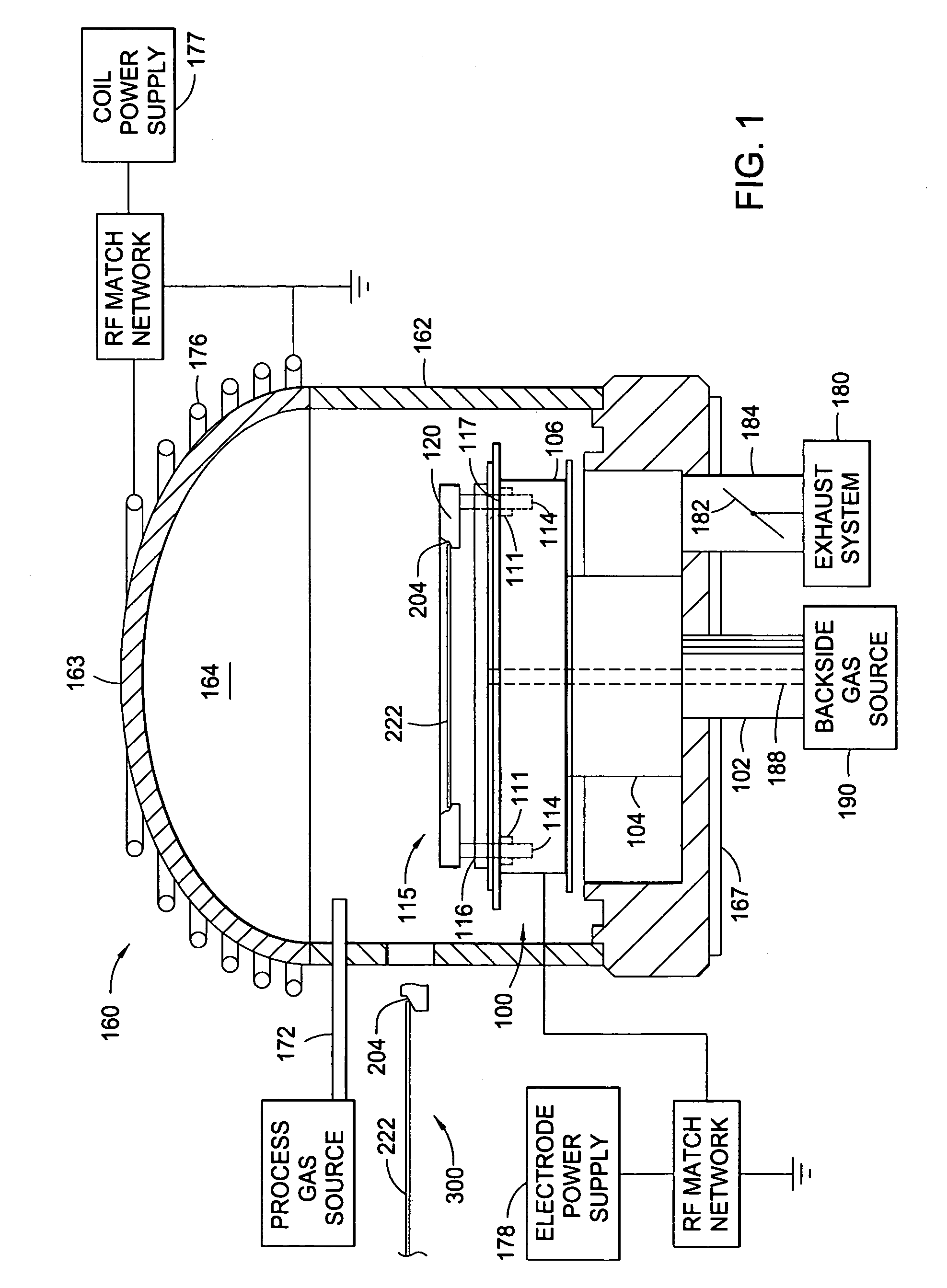
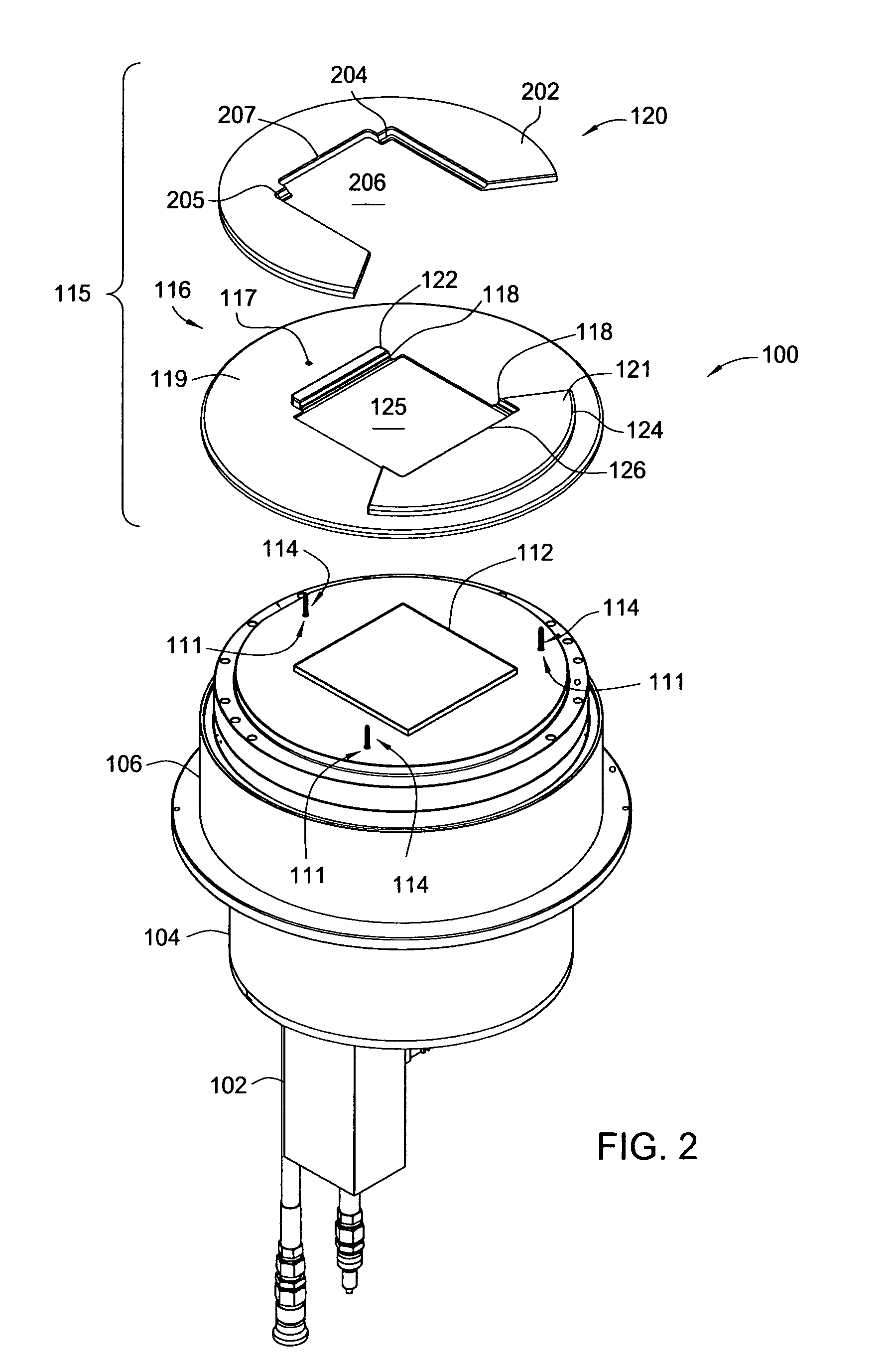
[0029]Aspects of the invention will be described below in reference to an inductively coupled plasma etch chamber. Suitable inductively coupled plasma etch chambers include the ETEC Tetra™ photomask etch chambers, such as the ETEC Tetra I™ photomask etch chamber and the ETEC Tetra II™ photomask etch chamber, available from ETEC of Hayward, Calif., or optionally, a Decoupled Plasma Source DPS™ processing chambers, such as the DPS I™, DPS II™, and DPS +™ processing chambers available from Applied Materials, Inc., of Santa Clara, Calif.

[0030]Other process chambers may be used including, for example, capacitively coupled parallel plate chambers and magnetically enhanced ion etch chambers, as well as inductively coupled plasma etch chambers of different designs. Examples of such suitable processing chambers are disclosed in U.S. patent application Ser. No. 09 / 325,026, filed on Jun. 3, 1999, which is incorporated by reference to the extent not inconsistent with the claims and disclosures ...


PUM

PropertyMeasurementUnit
feature sizesaaaaaaaaaa
angleaaaaaaaaaa

Abstract

Method and apparatus for supporting and transferring a substrate in a semiconductor wafer processing system are provided. In one aspect, an apparatus is provided for supporting a substrate comprising-a cover ring comprising a base having a bore disposed therethough, the base having an upper surface and one or more raised surfaces disposed adjacent the bore, wherein the raised surface comprise one or more first substrate support members disposed adjacent an edge of the bore and a capture ring disposed on the cover ring, the capture ring comprising a semi-circular annular ring having an inner perimeter corresponding to the bore of the cover ring and one or more second substrate support members disposed on the inner perimeter and adapted to receive a substrate, wherein the capture ring is adapted to mate with the cover ring and form one contiguous raised surface on the cover ring.

Description

BACKGROUND OF THE INVENTION[0001]1. Field of the Invention[0002]Embodiments of the present invention generally relate to a method and apparatus for supporting and transferring substrates during photomask fabrication.[0003]2. Description of the Related Art[0004]Semiconductor device geometries have dramatically decreased in size since such devices were first introduced several decades ago. Since then, integrated circuits have generally followed the two year / half-size rule (often called Moore's Law), which states that the number of devices on a chip doubles every two years. Today's fabrication plants are routinely producing devices having 0.35 μm and even 0.18 μm feature sizes, and tomorrow's plants soon will be producing devices having even smaller geometries.[0005]Increasing circuit densities have placed additional demands on processes used to fabricate semi-conductor devices. For example, as circuit densities increase, the widths of vias, contacts and other features, as well as the ...

Claims


Application Information

Patent Timeline
Patent Type & Authority Patents(United States)
IPC IPC(8): H01L21/306C23F1/00H01J37/32H01L21/687
CPCH01J37/321H01J37/32623H01L21/68707H01L21/68735
Inventor NGUYEN, KHIEMSATITPUNWAYCHA, PETERMAK, ALFRED W.
Owner APPLIED MATERIALS INC
Why Eureka
Try Eureka