

Method and apparatus for chemical mechanical polishing of semiconductor substrates
a technology of chemical mechanical polishing and semiconductor devices, applied in the direction of grinding machine components, manufacturing tools, lapping machines, etc., can solve the problems of difficult etching of copper and achieving precise patterns, affecting the functioning of semiconductor devices, and affecting the processing capacity, so as to improve the uniformity of polishing and improve the effect of planarization and removal of residual materials
- Summary
- Abstract
- Description
- Claims
- Application Information
AI Technical Summary
Benefits of technology
Problems solved by technology
Method used
Image

Examples
example
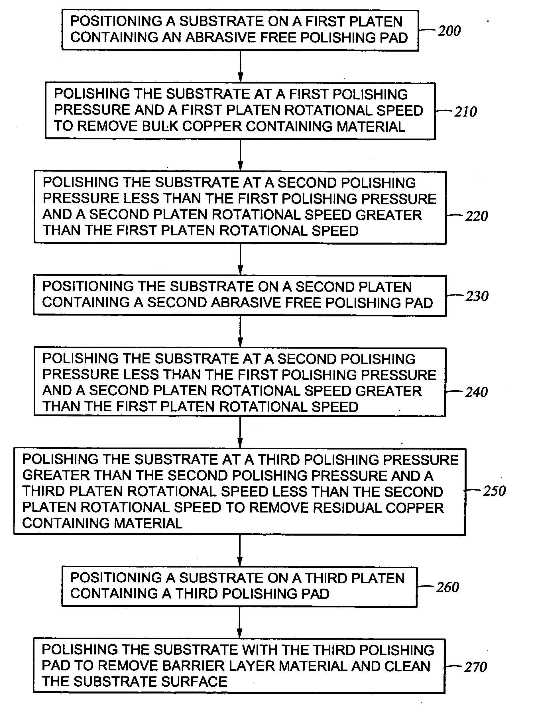
[0098] An example of a two-step copper polishing process according to aspects of the invention described herein is as follows. A substrate including a low k dielectric material, such as Black Diamond™ from Applied Materials, Inc. of Santa Clara, Calif., with feature definitions formed therein, a tantalum barrier layer deposited on the dielectric layer and in the feature definitions formed therein, and a copper-containing layer deposited on the barrier layer and filling the feature definitions formed therein is provided to the polishing apparatus disclosed above.
[0099] The substrate is positioned over an IC-1000 polishing pad of a first platen, and a first polishing composition of Cabot EPC-5001 is delivered to the polishing pad at a flow rate of about 200 ml / min. The platen is rotated at a platen rotational speed of about 800 cps (about 600 rpm) and a pressure of about 0.5 psi is applied between a substrate and polishing pad. The substrate is polished at this platen rotational spee...
PUM
| Property | Measurement | Unit |
|---|---|---|
| pressure | aaaaa | aaaaa |
| pressure | aaaaa | aaaaa |
| pressure | aaaaa | aaaaa |
Abstract
Description
Claims
Application Information