

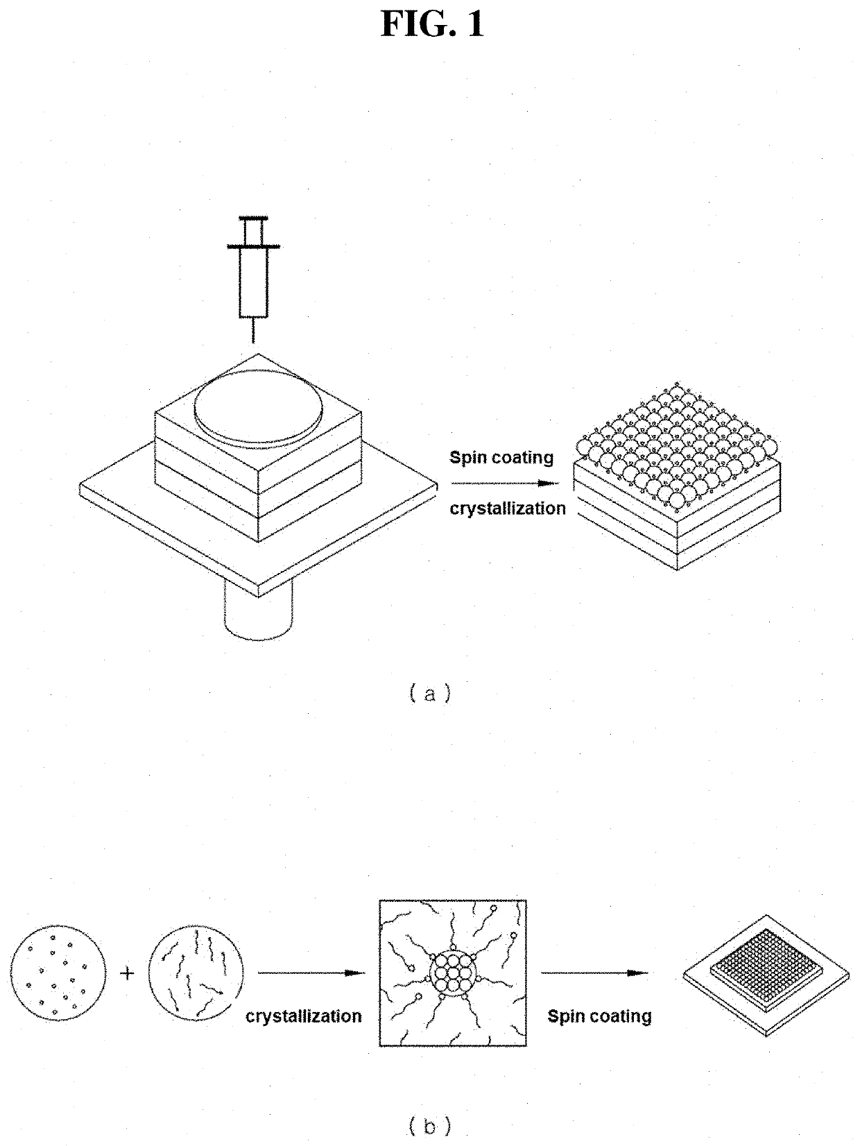
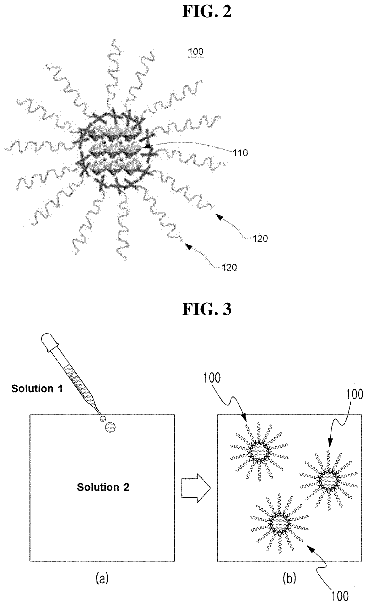
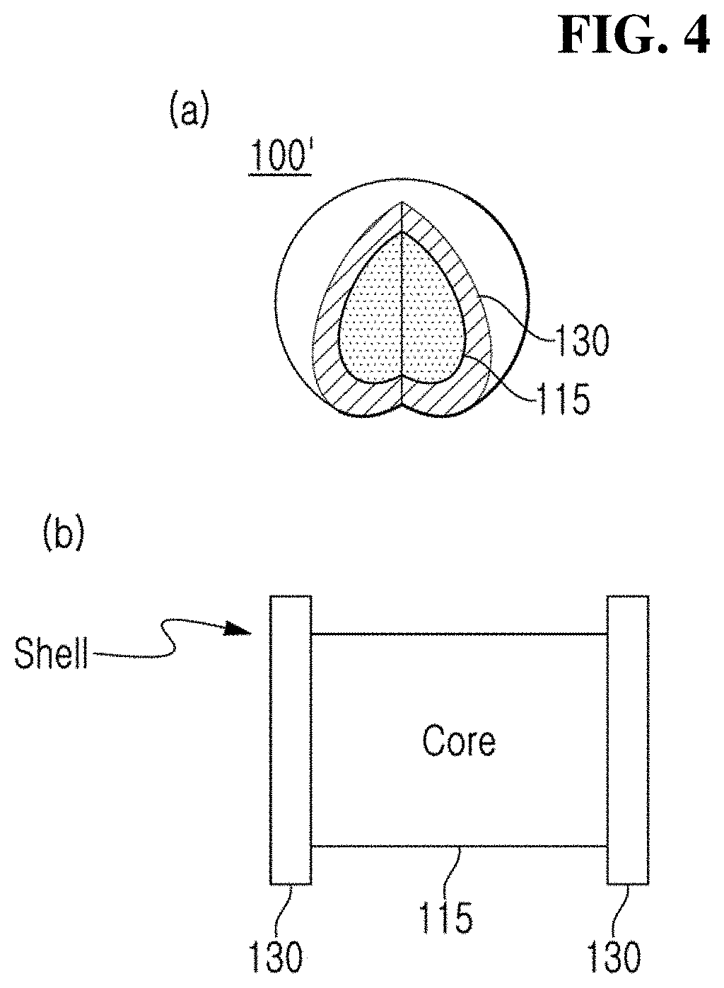
Defect suppressed metal halide perovskite light-emitting material and light-emitting diode comprising the same
a technology of metal halide perovskite and light-emitting diodes, which is applied in the direction of organic chemistry, lead halides, luminescent compositions, etc., can solve the problems of material limitations, color purity decline, poor color purity, etc., to enhance the photoluminescence lifetime and stability, and suppress the generation of defects inside the crystal
- Summary
- Abstract
- Description
- Claims
- Application Information
AI Technical Summary
Benefits of technology
Problems solved by technology
Method used
Image

Examples
embodiment 2-10
[1607]A perovskite nanoparticle solution and film were prepared in the same method as in Embodiment 1 except for using ethylammonium bromide, tert-butylammonium bromide, diethylammonium bromide, dimethylammonium bromide, ethane-1,2-diammonium bromide, imidazolium bromide, n-propylammonium bromide, iso-propylammonium bromide, and pyrrolidinium bromide instead of guanidinium bromide.
embodiment 11-30
[1608]A perovskite nanoparticle solution and film were prepared in the same method as in Embodiment 1-10 except for using methylammonium bromide and Cesium bromide instead of formamidinium bromide.
Fabrication of Red Light-Emitting Metal Halide Perovskite Nanoparticle Solution and Film
[1609]A precursor solution was prepared by dissolving a metal halide perovskite in a polar solvent. At this time, as the polar solvent, dimethylformamide was used, and as a metal halide perovskite precursor, formamidinium iodide (FAI), guanidinium iodide (GAI), PbI2 was used. At this time, the ratio of (FAI+GAI) and PbI2 is 2:1, and by adjusting the mixing ratio of FAI and GAI, the composition of GAI contained in metal halide perovskite nanoparticles can be adjusted.
[1610]The mixing ratio of GAI to the total amount of FAI and GAI is 5%, 6%, 7%, 8%, 9%, 10%, 11%, 12%, 13%, 14%, 15%, 16%, 17%, 18%, 19%, 20%, 22%, 24%, 26%, 28%, 30%, 32%, 34%, 36%, 38%, 40%, 45%, 50%, 55%, 60%, 80%, 100%
[1611]Thereafter, ...
embodiment 32-40
[1614]A perovskite nanoparticle solution and film were prepared in the same method as in Embodiment 31 except for using ethylammonium iodide, tert-butylammonium iodide, diethylammonium iodide, dimethylammonium iodide, ethane-1,2-diammonium iodide, imidazolium iodide, n-propylammonium iodide, iso-propylammonium iodide, and pyrrolidinium iodide instead of guanidinium iodide.
PUM
| Property | Measurement | Unit |
|---|---|---|
| exciton Bohr diameter | aaaaa | aaaaa |
| structure | aaaaa | aaaaa |
| ionic radius | aaaaa | aaaaa |
Abstract
Description
Claims
Application Information