CMOS well structure and method of forming the same

a well and cmos technology, applied in the field of integrated semiconductor devices, can solve the problems of not being able to isolate the n-well and biasing it differently from the substrate, not being able to apply the same scaling factor which applies to the transistor to the conventional well, and not being able to uniformly measure the doping profile at the edges of the well across the breadth

Active Publication Date: 2006-11-07
GLOBALFOUNDRIES U S INC
View PDF5 Cites 98 Cited by
  • Summary
  • Abstract
  • Description
  • Claims
  • Application Information

AI Technical Summary

Problems solved by technology

In this case, for example, when an n-well is formed in an n-type substrate, unless the bottom and the surrounding of the n-well is sealed by p-dopant material, it is not possible to isolate the n-well and bias it differently from the substrate.
A great challenge in well formation has been experienced as CMOS technology is scaled beyond deep sub-micron and into the nanometer groundrule regime.
However, the same scaling factors which apply to the transistor may not apply to conventional wells which are formed by ion implantation.
One problem associated with using ion implantation to form wells is the well proximity effect, wherein the doping profile at the edges of a well is not uniform across the breadth of the well.
However, this approach is not suitbale in a 6-T SRAM array where memory cells must be closely packed.
Specifically, keeping devices away from the edges of wells obviously wastes chip space, and if the resultant threshold voltage is unacceptable to the SRAM cell, then an additional mask must be added to the process to properly center the threshold voltage, resulting in additional cost and complexity.

Method used


Image

  • CMOS well structure and method of forming the same
  • CMOS well structure and method of forming the same
  • CMOS well structure and method of forming the same

Examples


Embodiment Construction

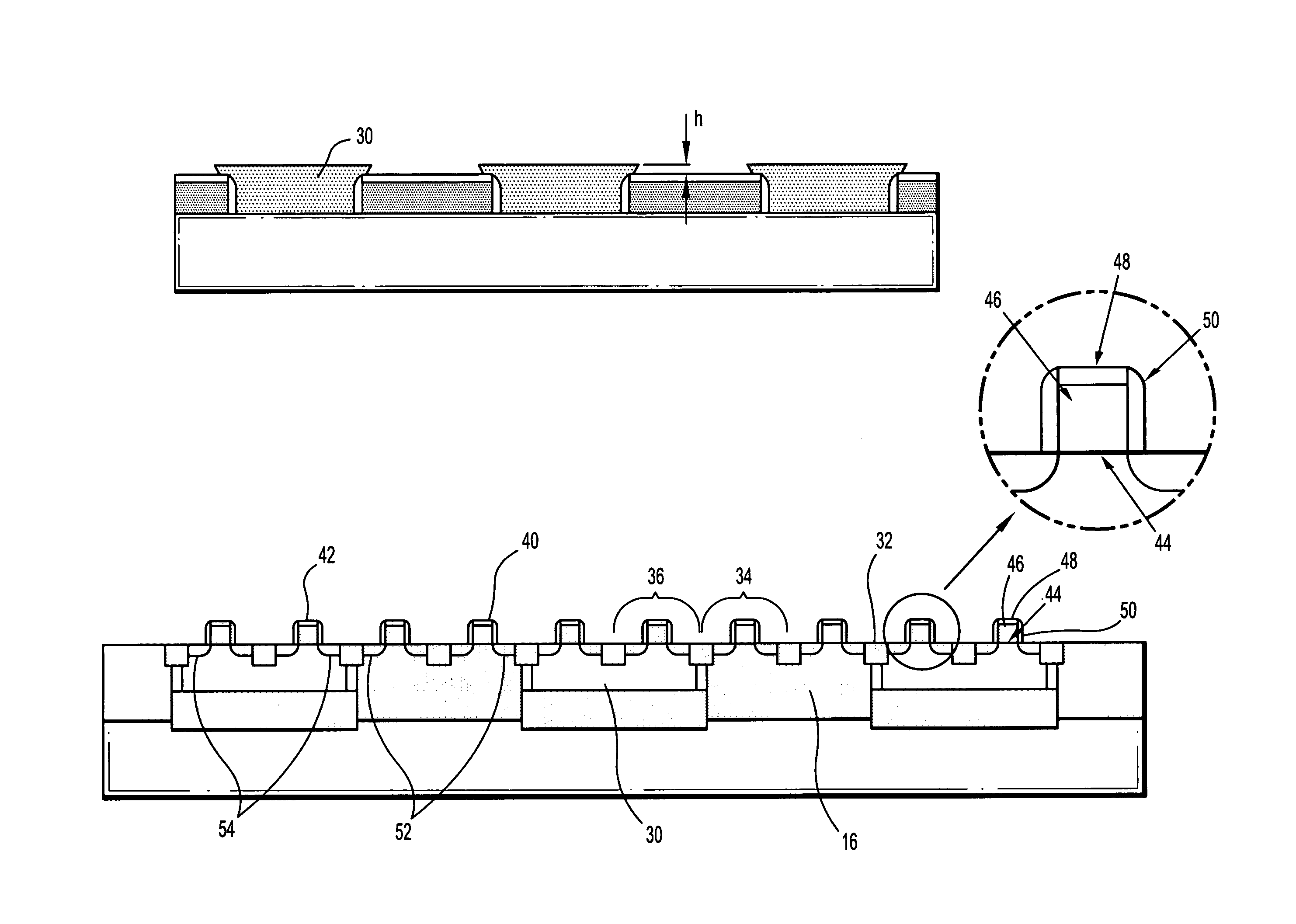
[0018]In various exemplary embodiments of the invention, a vertical sidewall well is formed in a bulk silicon wafer. Consecutive low-temperature selective epitaxy processes are used to form the vertical sidewall single well, double well and triple well structures, so that proximity effect due to ion scattering is eliminated. In the absence of the proximity effect, minimum distance can be kept between devices all the way to the well boundary. The various exemplary embodiments of the invention use both deep and shallow trench isolation. Spacer-type thin vertical deep trenches are formed at the boundary of the wells using side-wall spacer techniques, while the shallow trenches are used not only to isolate the devices within the wells, but also to remove defects at the well boundary caused by selective epitaxy.

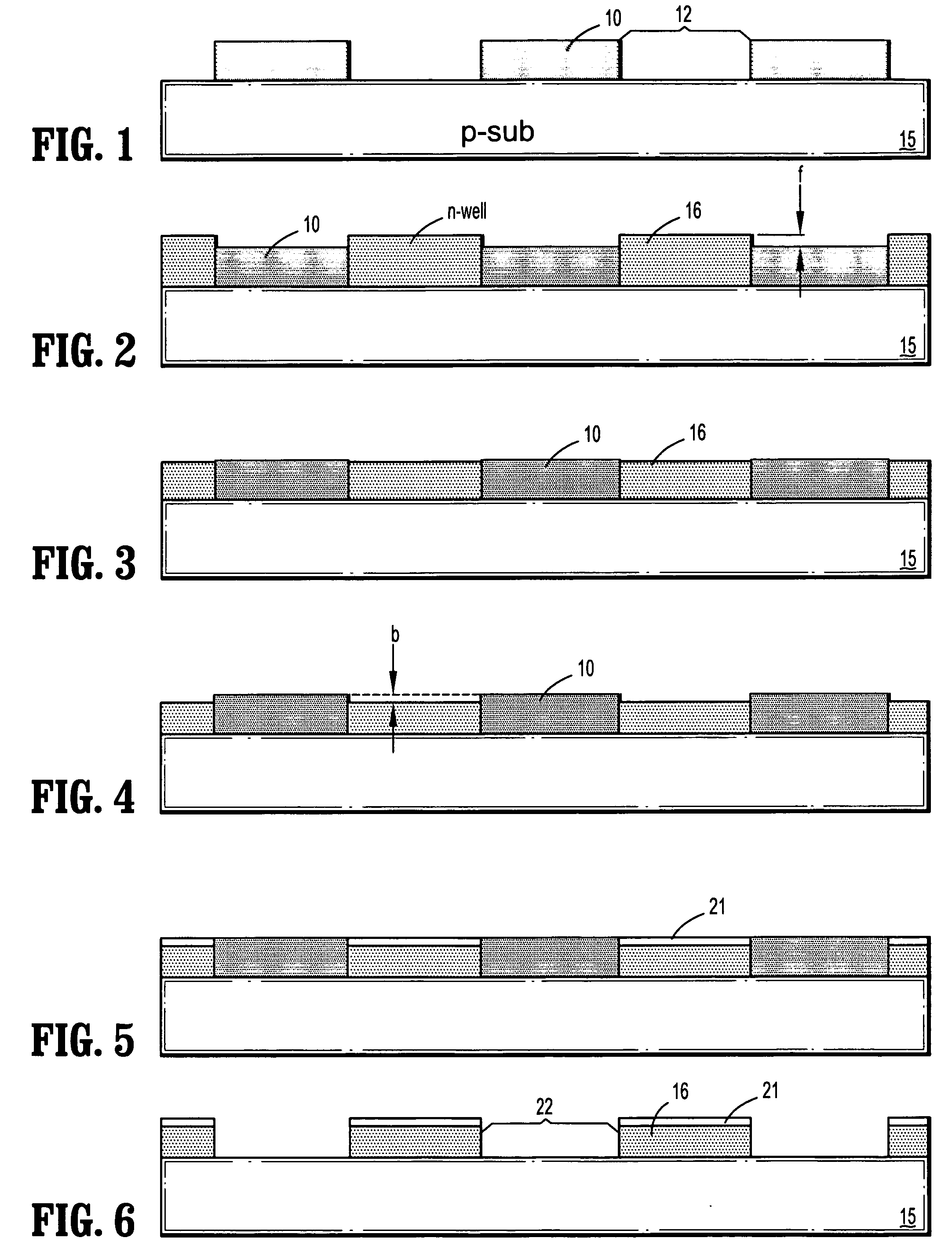
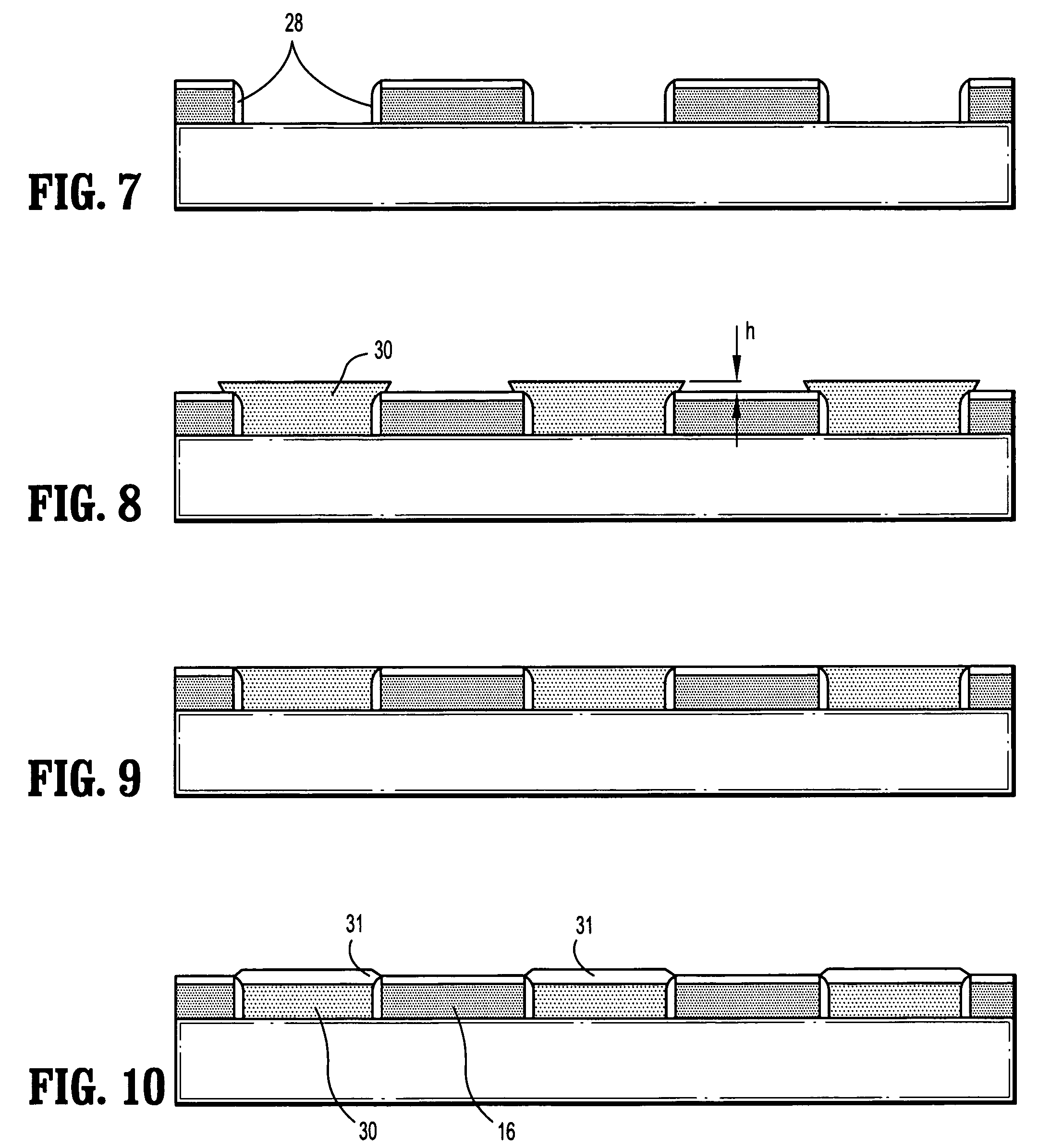
[0019]FIGS. 1–11 are cross sectional views showing various steps of a method for forming a CMOS structure according to an exemplary embodiment of the invention. The present embodi...


PUM


Abstract

A method for forming a CMOS well structure including forming a plurality of first conductivity type wells over a substrate, each of the plurality of first conductivity type wells formed in a respective opening in a first mask. A cap is formed over each of the first conductivity type wells, and the first mask is removed. Sidewall spacers are formed on sidewalls of each of the first conductivity type wells. A plurality of second conductivity type wells are formed, each of the plurality of second conductivity type wells are formed between respective first conductivity type wells. A plurality of shallow trench isolations are formed between the first conductivity type wells and second conductive type wells. The plurality of first conductivity type wells are formed by a first selective epitaxial growth process, and the plurality of second conductivity type wells are formed by a second selective epitaxial growth process.

Description

BACKGROUND OF THE INVENTION[0001]1. Field of the Invention[0002]The present invention relates to semiconductor devices, and more particularly to integrated semiconductor devices, such as complementary metal oxide semiconductor (CMOS) devices.[0003]2. Description of the Related Art[0004]In CMOS integration, i.e. NMOS and PMOS on the same chip, at least one well is needed on a silicon substrate. For example, when using a p-type substrate, NMOS can be fabricated on the substrate, while PMOS must be fabricated on an n-well in the substrate. Alternatively, when using an n-type substrate, PMOS can be fabricated on the substrate, while NMOS must be fabricated on a p-well in the substrate. Further, in order to avoid problems associated with latch-up, a dual-well approach is usually employed. The dual-well approach involves forming NMOS on a p-well and PMOS on an n-well, regardless of the type of starting substrate. The dopant concentrations of both wells are tailored so that the latch-up si...

Claims


Application Information

Patent Timeline
Patent Type & Authority Patents(United States)
IPC IPC(8): H01L21/8238H01L21/76H01L27/08H01L27/092H01L29/78
CPCH01L21/823892H01L29/78H01L27/0928H01L21/02293H01L21/041H01L21/67075H01L21/76876H01L21/8238H01L21/823842H01L29/66719H01L29/7846
Inventor HAENSCH, WILFRIEDHOOK, TERENCE B.HSU, LOUIS C.JOSHI, RAJIV V.RAUSCH, WERNER
Owner GLOBALFOUNDRIES U S INC
Why Eureka
Try Eureka