Method for generating a synchronization signal based on the clock ratio between two clock domains for data transfer between the domains

a clock domain and clock domain technology, applied in the field of microprocessors, can solve the problems of failure of functional testing, chip failure, and inability to produce actual operation conditions

Active Publication Date: 2006-11-07
ORACLE INT CORP
View PDF13 Cites 27 Cited by
  • Summary
  • Abstract
  • Description
  • Claims
  • Application Information

AI Technical Summary

Benefits of technology

[0010]In another embodiment, an apparatus configured to communicate data across different frequency domains is provided. The apparatus includes a first storage cell operating at a first clock frequency and a second storage cell operating at a second clock frequency. The second storage cell is designed to receive an output of the first storage cell. The apparatus includes synchronizing signal circuitry associated with the second storage cell. The synchronizing signal circuitry is configured to control acceptance of the output of the first storage cell through a synchronizing signal. The synchronizing signal correlates the second clock frequency to the first clock frequency in order to define a window for communicating data between the first storage cell and the second storage cell.
[0011]In still yet another embodiment, an electronic system is provided. The system includes a microchip having a first region operating at a first clock speed and a second region operating at a second clock speed. The microchip includes a first storage cell operating at the first clock speed and a second storage cell operating at the second clock speed. The second storage cell is designed to receive an output of the first storage cell. Synchronizing signal circuitry associated with the second storage cell is provided. The synchronizing signal circuitry is configured to control acceptance of the output of the first storage cell through a synchronizing signal. The synchronizing signal correlates the second clock speed to the first clock speed in order to define a window for communicating data between the first storage cell and the second storage cell. Logic for generating values provided to the first and second storage cells is included.

Problems solved by technology

However, this does not produce the actual functionality of operating conditions as the timing of events are being changed.
Therefore, the chip may pass during the system debug but fail during functional testing.
Another shortcoming of this technique is the relatively high overhead and transfer latency associated with the technique.

Method used


Image

  • Method for generating a synchronization signal based on the clock ratio between two clock domains for data transfer between the domains
  • Method for generating a synchronization signal based on the clock ratio between two clock domains for data transfer between the domains
  • Method for generating a synchronization signal based on the clock ratio between two clock domains for data transfer between the domains

Examples


Embodiment Construction

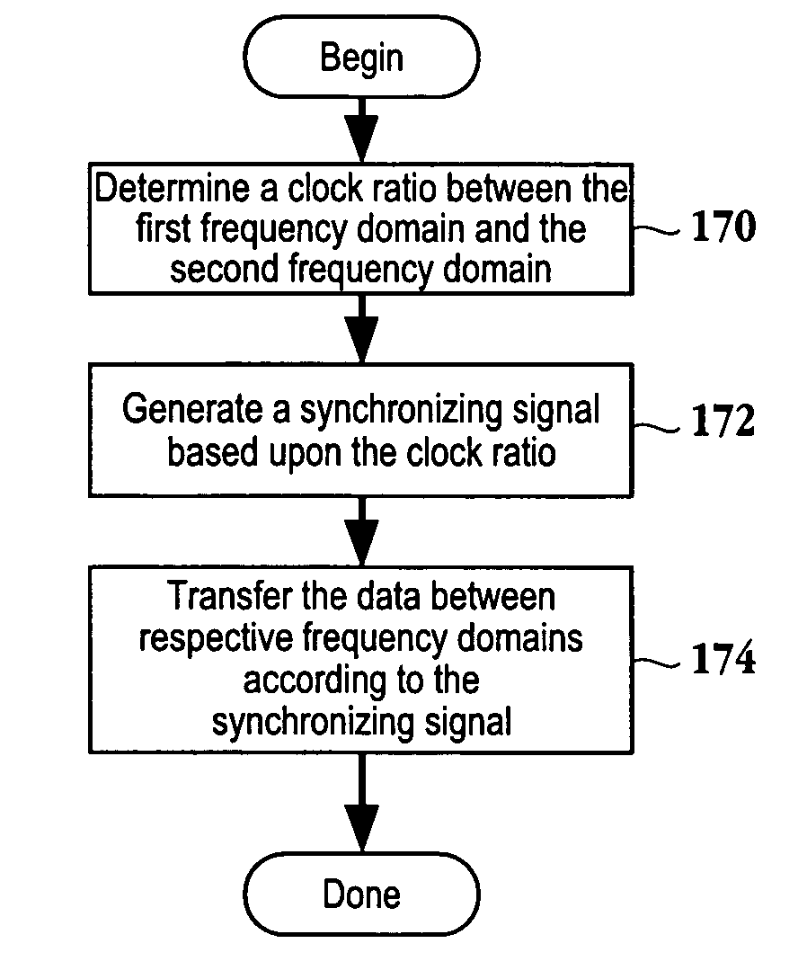
[0021]An invention is described for a system, device and method for efficiently transferring data across different clock frequency domains. It will be obvious, however, to one skilled in the art, that the present invention may be practiced without some or all of these specific details. In other instances, well known process operations have not been described in detail in order not to unnecessarily obscure the present invention. The term about as used to herein refers to + / −10% of the referenced value.

[0022]The embodiments of the present invention provide a system, device and method enabling the transfer of data across different clock frequencies in a deterministic manner that minimizes overhead. The deterministic manner allows for the elimination of special test circuitry that forces the clocks frequencies to act in a certain manner during system debug, e.g., scan testing. Accordingly, the system or chip behaves in the same manner during debug operations as during functional perform...


PUM


Abstract

A method for communicating across first and second frequency domains of an integrated microchip is provided. The method initiates with determining a clock ratio between the first frequency domain and the second frequency domain. The first frequency domain is associated with a faster clock cycle. Then, a synchronizing signal based upon the clock ratio is generated. The synchronizing signal coordinates communication of data between the first and second frequency domains. Next, the data is transferred between respective frequency domains according to the synchronizing signal. A microchip and a system enabling synchronous data transfer across different frequency domains are also provided.

Description

BACKGROUND OF THE INVENTION[0001]1. Field of the Invention[0002]The present invention relates generally to microprocessors, and more specifically to a method and apparatus for the transfer of data across disparate within a micro-chip.[0003]2. Description of the Related Art[0004]In a multi-processor environment, it is important to transmit data between processors. For example, system on a chip (SoC) technology enables the packaging of all the parts and electronic circuits for a system on an integrated circuit. This technology may be used for cell phones, digital cameras, and other consumer electronics. Here, multiple processors may be in communication with each other. The highly integrated micro-chips operate various parts of the chip at different frequencies. The conventional approach to the communication across different frequency domains is to treat each clock as completely independent and the interface as completely asynchronous.[0005]FIG. 1 is a simplified schematic of an appara...

Claims


Application Information

Patent Timeline
Patent Type & Authority Patents(United States)
IPC IPC(8): G06F1/04G06F1/12G06F13/00
CPCG06F1/12G06F13/42
Inventor SHARMA, ANUP K.KRISHNASWAMY, VENKATRAM
Owner ORACLE INT CORP
Why Eureka
Try Eureka