Array of cells including a selection bipolar transistor and fabrication method thereof

a technology of selection bipolar transistor and array, which is applied in the direction of transistors, electrical devices, semiconductor devices, etc., can solve the problems that the optimization of the layout of the memory cell in the prior application does not take into account the optimization of the memory cell layout, and achieve the effect of increasing the compactness of the array

Active Publication Date: 2006-11-14
OVONYX MEMORY TECH LLC
View PDF13 Cites 6 Cited by
  • Summary
  • Abstract
  • Description
  • Claims
  • Application Information

AI Technical Summary

Benefits of technology

[0011]To increase the compactness of the array, according to one aspect of the invention, at least two cells are housed in a same active area of the device.

Problems solved by technology

This prior application however does not deal with the optimization of the layout of the memory cell.

Method used


Image

  • Array of cells including a selection bipolar transistor and fabrication method thereof
  • Array of cells including a selection bipolar transistor and fabrication method thereof
  • Array of cells including a selection bipolar transistor and fabrication method thereof

Examples


Embodiment Construction

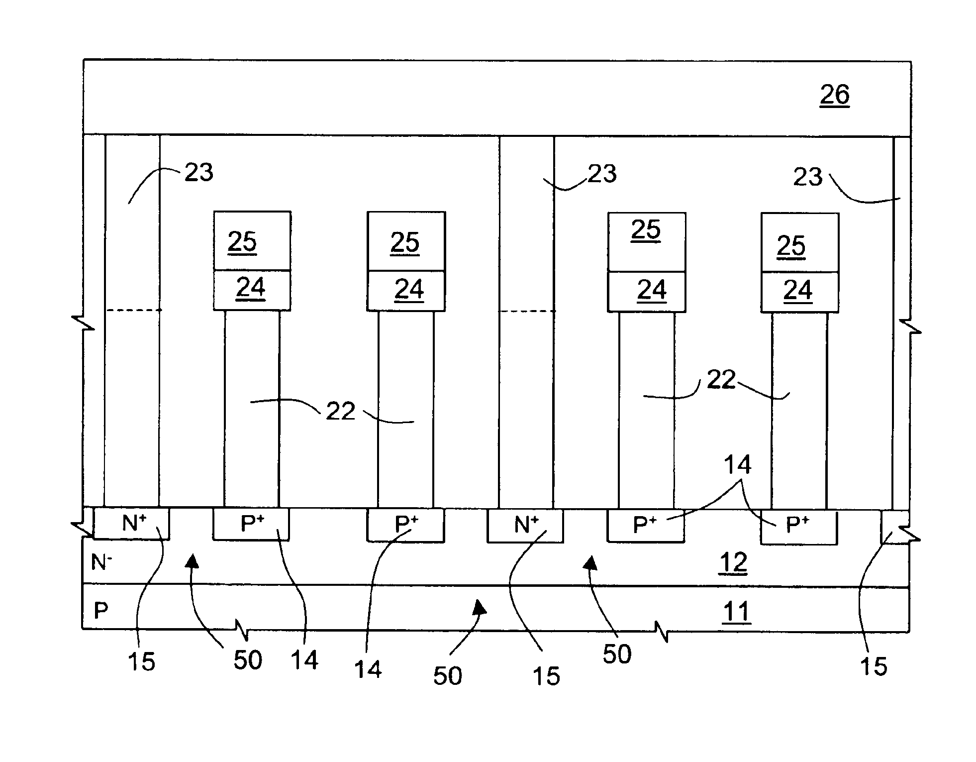
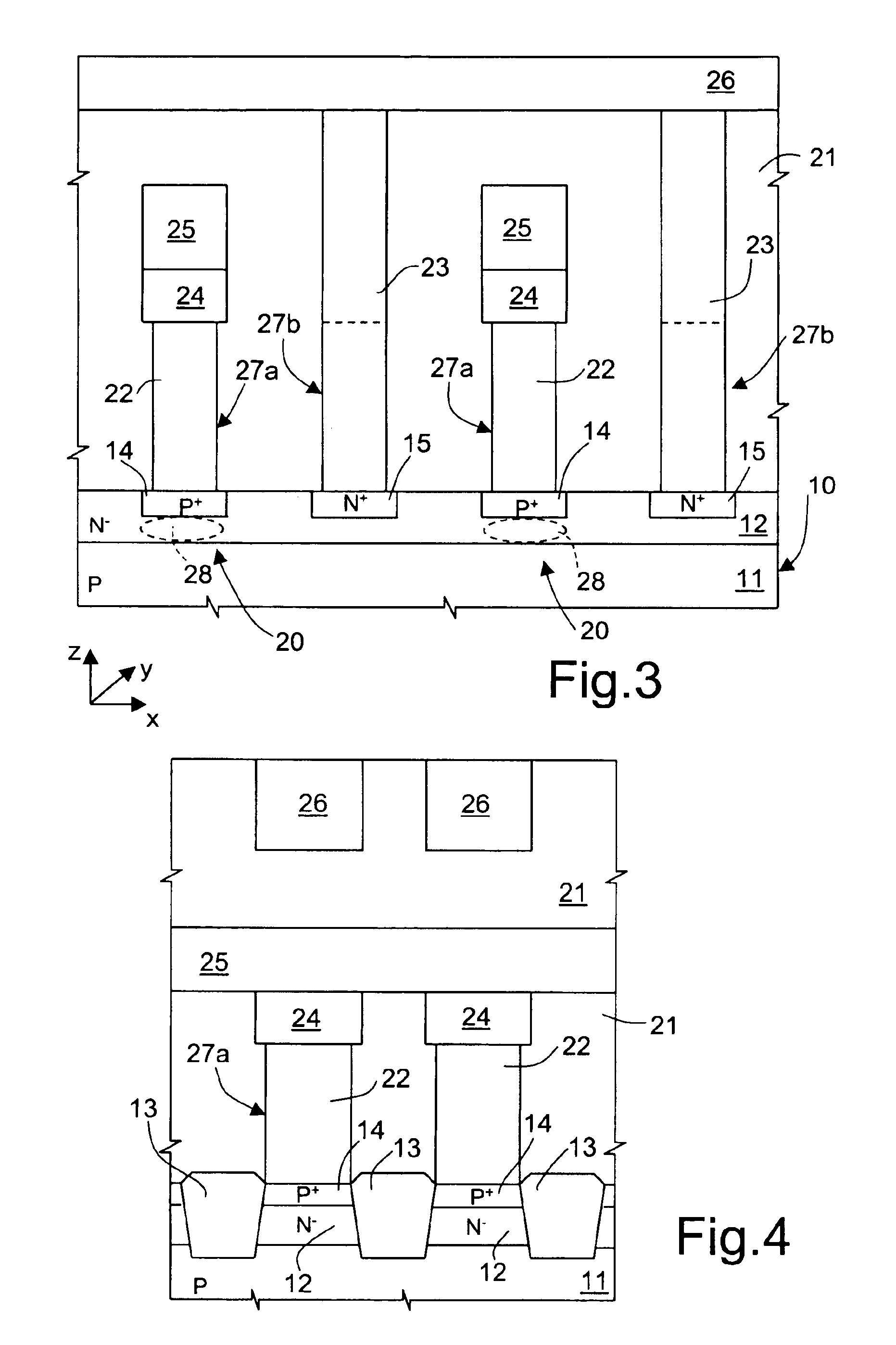
[0024]According to the embodiment of FIGS. 2-4, a memory array is formed in a body 10 of semiconductor material including a P-type common collector region 11. As visible in particular from FIG. 4, the body 10 houses a plurality of active area strips 12, of N-type, defining base regions. The active area strips 12 extend parallel to each other along a first direction (X-direction) and are electrically insulated from each other by field oxide regions 13 (FIG. 4).

[0025]Each active area strip 12 accommodates a plurality of emitter regions 14, of P+-type, and plurality of base contact regions 15, of N+-type, that are arranged alternately, that is each emitter region 14 is arranged between two base contact regions 15, and each base contact region 15 is arranged between two emitter regions 14. Thus, each pair of regions including an emitter region 14 and the adjacent base contact region 15 (for example, an emitter region 14 and the base contact region 15 arranged on right thereof, the activ...


PUM


Abstract

A cell array is formed by a plurality of cells each including a selection bipolar transistor and a storage component. The cell array is formed in a body including a common collector region of P type; a plurality of base regions of N type, overlying the common collector region; a plurality of emitter regions of P type formed in the base regions; and a plurality of base contact regions of N type and a higher doping level than the base regions, formed in the base regions, wherein each base region is shared by at least two adjacent bipolar transistors.

Description

BACKGROUND OF THE INVENTION[0001]1. Field of the Invention[0002]The present invention relates to an array of cells including a selection bipolar transistor and a fabrication method thereof. In particular, the invention refers to a cell array of a phase change memory (PCM) device, without being limited thereto.[0003]2. Description of the Related Art[0004]As is known, phase change memory cells utilize a class of materials that have the unique property of being reversibly switchable from one phase to another with measurable distinct resistivity. Specific materials that may be suitably used in phase change memory cells are alloys of elements of the VI group of the periodic table as Te or Se, also called chalcogenides or chalcogenic materials. Thus a thin film of chalcogenic material may be employed as a programmable resistor, switching between a high and a low resistance condition.[0005]The use of chalcogenic storage elements has been already proposed to form a memory cell. To avoid dis...

Claims


Application Information

Patent Timeline
Patent Type & Authority Patents(United States)
IPC IPC(8): H01L27/102H01L27/10H01L27/24H01L29/68
CPCH01L27/101H01L27/2445H01L27/2463H01L29/685H01L45/06H01L45/1233H10B63/32H10B63/80H10N70/231H10N70/826
Inventor PELLIZZER, FABIOCASAGRANDE, GIULIOBEZ, ROBERTO
Owner OVONYX MEMORY TECH LLC
Why Eureka
Try Eureka