Programmable routing structures providing shorter timing delays for input/output signals

Inactive Publication Date: 2006-11-14
ALTERA CORP
View PDF8 Cites 153 Cited by
  • Summary
  • Abstract
  • Description
  • Claims
  • Application Information

AI Technical Summary

Benefits of technology

[0008]The present invention provides techniques for routing signals to and from input/output pads on a programmable chip that reduce signal delay times. Programmable routing conductors are provided that are dedicated to routing sig

Problems solved by technology

As applications for PLDs have become more complex, customers have continue to demand more logic blocks on each PLD die.
However, signal delay

Method used


Image

  • Programmable routing structures providing shorter timing delays for input/output signals
  • Programmable routing structures providing shorter timing delays for input/output signals
  • Programmable routing structures providing shorter timing delays for input/output signals

Examples


Example

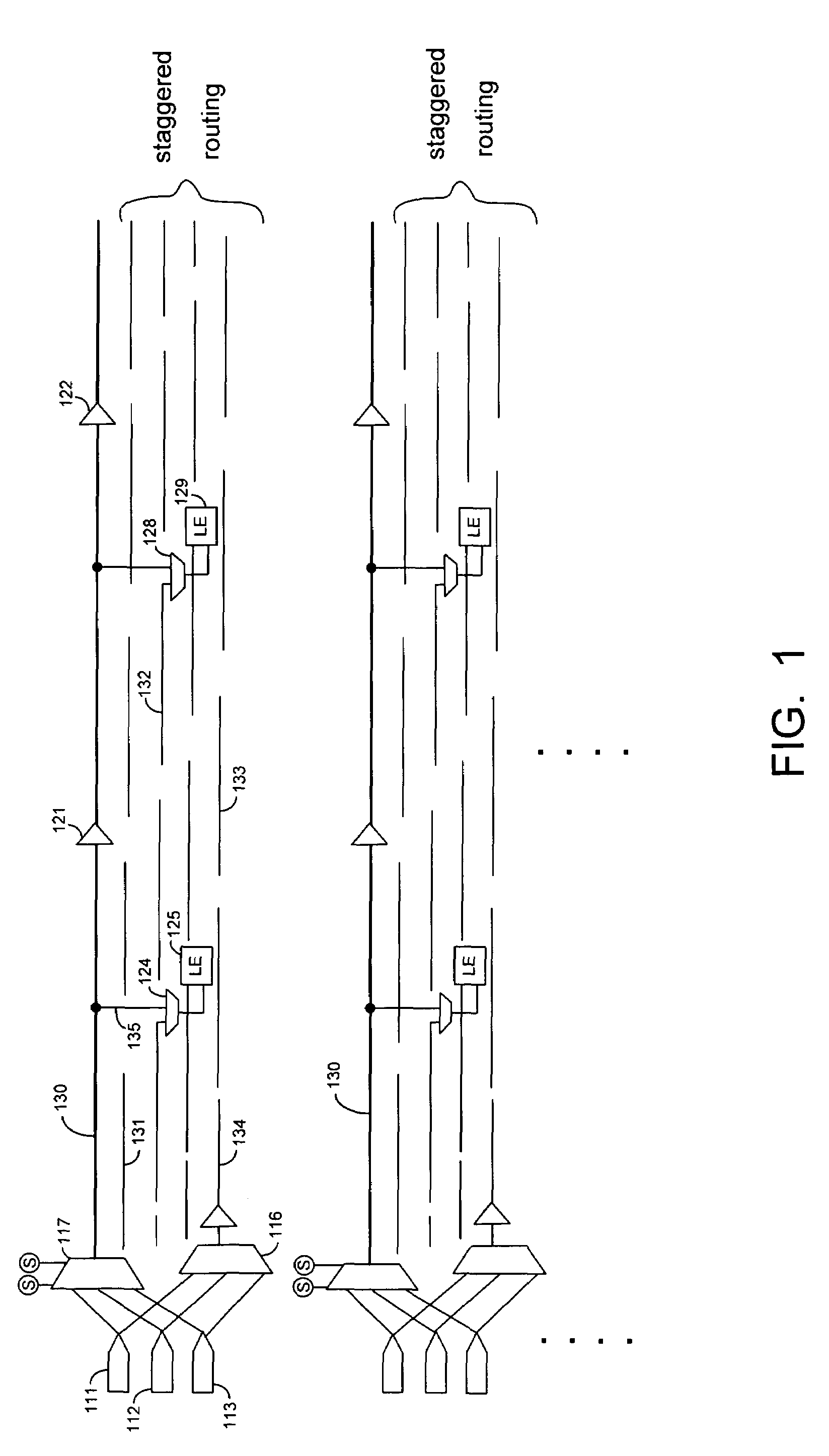
[0017]FIG. 1 illustrates a dedicated input routing structure according to a first embodiment of the present invention. Programmable horizontal routing conductors 130 are dedicated for transmitting signals from input pads of a programmable logic integrated circuit (IC). Input pads 111, 112, and 113 are examples of input pads on the IC.

[0018]Input signals applied to any of pads 111–113 can be driven to one of routing conductors 130 through 3:1 multiplexer 117. Multiplexer 117 couples conductor 130 to one of pads 111–113 in response to the states of two select signals. The select signals (shown as S in FIG. 1) are stored in memory. Signals driven along line 130 are amplified by buffers 121 and 122. Buffers 121 and 122 (and other buffers) can be inverting or non-inverting buffers.

[0019]The programmable logic integrated circuit includes staggered horizontal routing conductors such as conductors 131, 132, 133, and 134 shown in FIG. 1. The staggered routing conductors can include local and...

Example

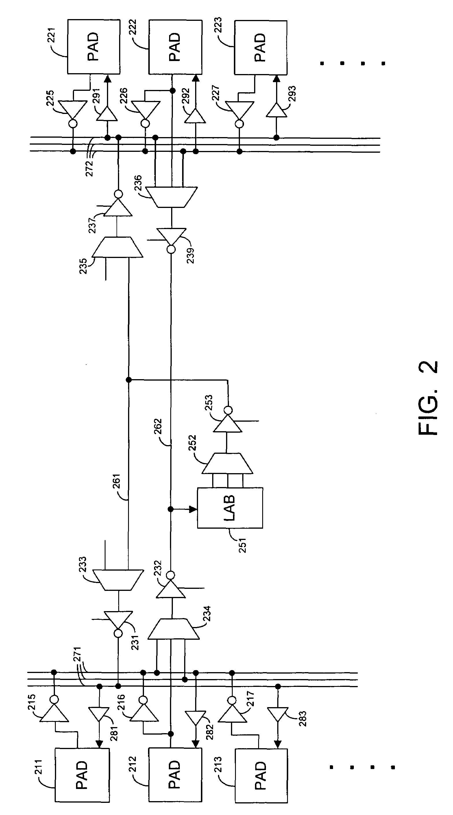
[0022]FIG. 2 illustrates a dedicated I / O routing structure according to a second embodiment of the present invention. FIG. 2 illustrates a portion of a programmable logic IC. The IC includes vertical routing conductors 271–272 and horizontal routing conductors 261–262 that are dedicated for routing signals to and from I / O pads such as pads 211–213 and 221–223. Although a limited number of dedicated I / O routing conductors are shown in FIG. 2, embodiments of the present invention can include any number of vertical and horizontal dedicated I / O routing conductors arranged in any suitable configuration.

[0023]Input signals applied to pads 211–213 are driven to dedicated I / O conductors 271 through inverting buffers 215–217, respectively. One of conductors 271 can be programmably coupled to horizontal conductor 262 through multiplexer 234 and tristate driver 232. Also, an input signal applied to pad 212 can be driven directly to conductor 262 through multiplexer 234 without being routed thr...

Example

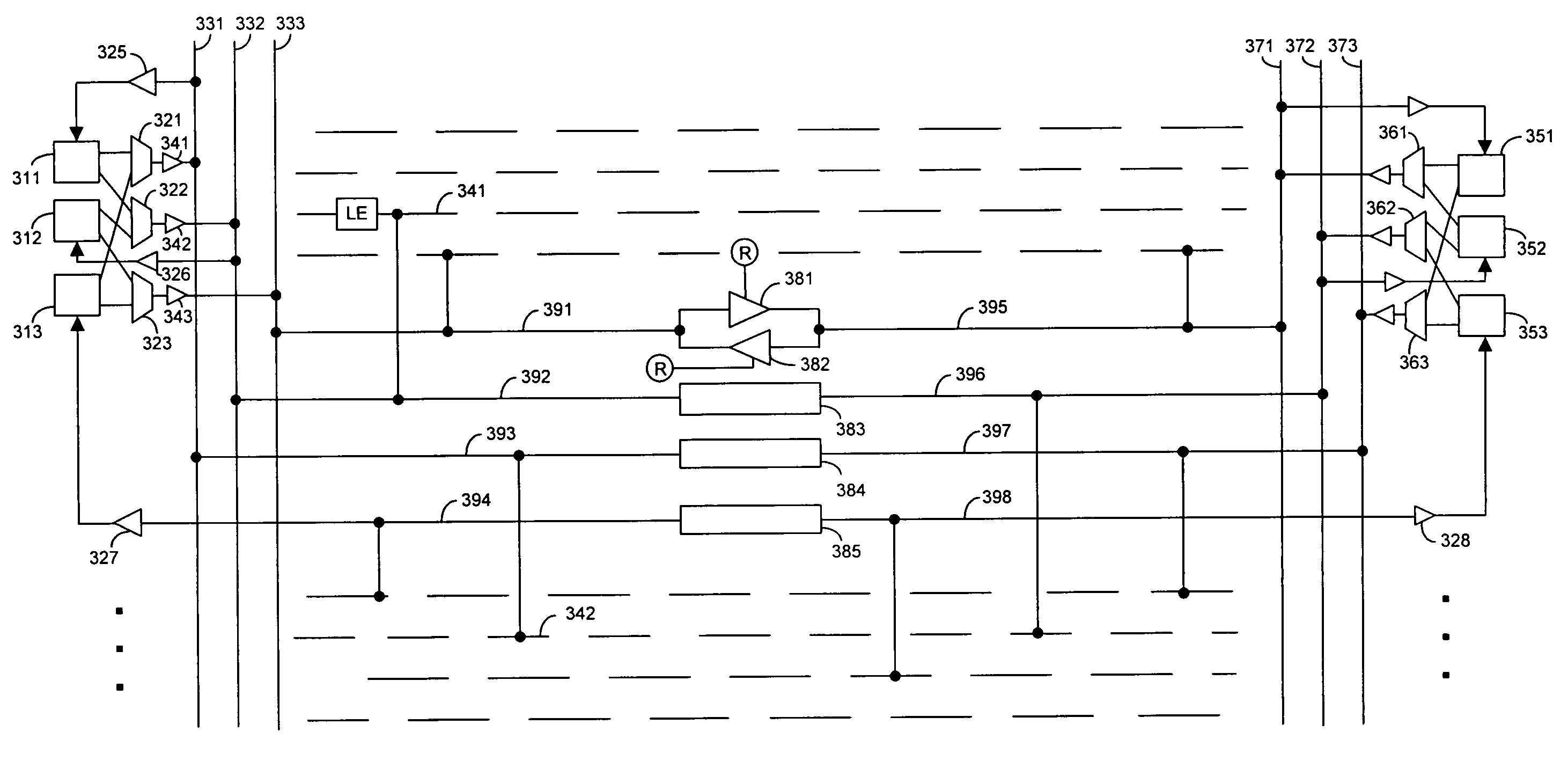
[0034]FIG. 3 illustrates another dedicated I / O routing structure according to a third embodiment of the present invention. The embodiment of FIG. 3 also has a limited number of dedicated I / O conductors. The dedicated I / O routing structure of FIG. 3 includes vertical conductors 331–333 and 371–373 and horizontal conductors 391–398.

[0035]Input signals applied to I / O pads 311–313 can be routed to vertical conductors 331–333 as will now be discussed. 2:1 multiplexers 321–323 are controlled by RAM bits that are transmitted to select inputs (not shown) of the multiplexers. Each multiplexer 321–323 has two inputs coupled to two pads and a single output coupled to one of conductors 331–333. Tristate drivers 341–343 are coupled between the output of multiplexers 321–323 and conductors 331–333, respectively.

[0036]An input signal applied to a particular I / O pad can be driven to one or two (but not three) of conductors 331–333. For example, an input signal applied to pad 311 can be driven to co...


PUM


Abstract

Techniques are provided for routing signals to and from input/output pads on a programmable chip that reduce signal delay times. A programmable routing structure is provided that is dedicated to routing signals to and from the input/output (I/O) pads. The programmable routing structure can include long conductors that transmit signals across the chip quickly without the delay encountered in shorter routing conductors. Signals can be routed to and from the I/O pads through vertical and horizontal dedicated routing conductors that bypass global routing conductors. The dedicated I/O routing structure allows signals to be driven onto the chip and off chip more quickly can be achieved through standard programmable routing structures. The dedicated I/O routing structure can be depopulated to reduce the number of programmable connections between the individual conductors, decreasing die area requirements.

Description

BACKGROUND OF THE INVENTION[0001]The present invention relates to programmable routing structures that provide fast paths for input / output signals, and more particularly, to a programmable routing structures that reduce delay for signals driven to and from input / outputs pads of an integrated circuit.[0002]Programmable logic integrated circuits (ICs) can be configured to perform a variety of user functions. Programmable logic ICs include programmable logic devices (PLDs), field programmable gate arrays (FPGAs), programmable logic arrays (PLAs), etc. Programmable logic ICs typically have numerous logic blocks (also called logic elements) that can be configured to implement various combinatorial and sequential functions.[0003]The logic blocks have access to a programmable interconnect structure. The programmable interconnect structure can be programmed to interconnect the logic blocks in almost any desired configuration. Logic blocks are often grouped into logic array blocks or macroce...

Claims


Application Information

Patent Timeline
IPC IPC(8): H03K19/177G06F7/38H01L25/00
CPCH01L27/0207H01L27/11898H03K19/17744
Inventor HUTTON, MICHAEL D.LEWIS, DAVID
Owner ALTERA CORP
Why Eureka
Try Eureka