Array substrate, manufacturing method thereof, and display device

A technology of array substrates and conductive structures, which is applied in semiconductor/solid-state device manufacturing, semiconductor devices, electrical components, etc., can solve the problems that display devices cannot display images normally, and achieve the effect of improving the display images that cannot be displayed normally

Active Publication Date: 2018-11-30
BOE TECH GRP CO LTD +1
View PDF3 Cites 0 Cited by
  • Summary
  • Abstract
  • Description
  • Claims
  • Application Information

AI Technical Summary

Problems solved by technology

[0005] The purpose of the present invention is to provide an array substrate and its manufacturing method, and a display device, which can improve the problem that the display device cannot display images normally due to signal delay

Method used


Image

  • Array substrate, manufacturing method thereof, and display device
  • Array substrate, manufacturing method thereof, and display device
  • Array substrate, manufacturing method thereof, and display device

Examples


Embodiment 1

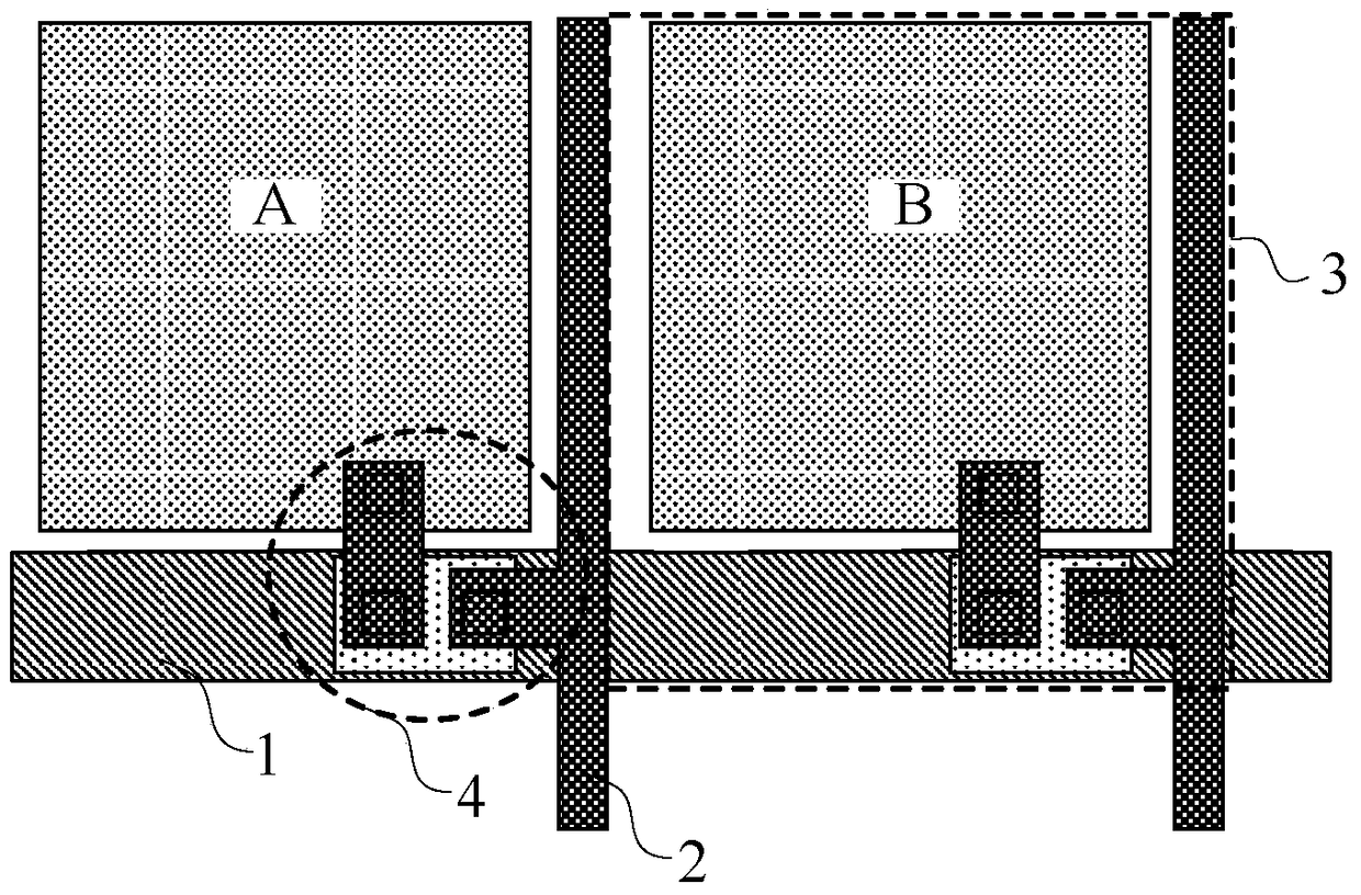
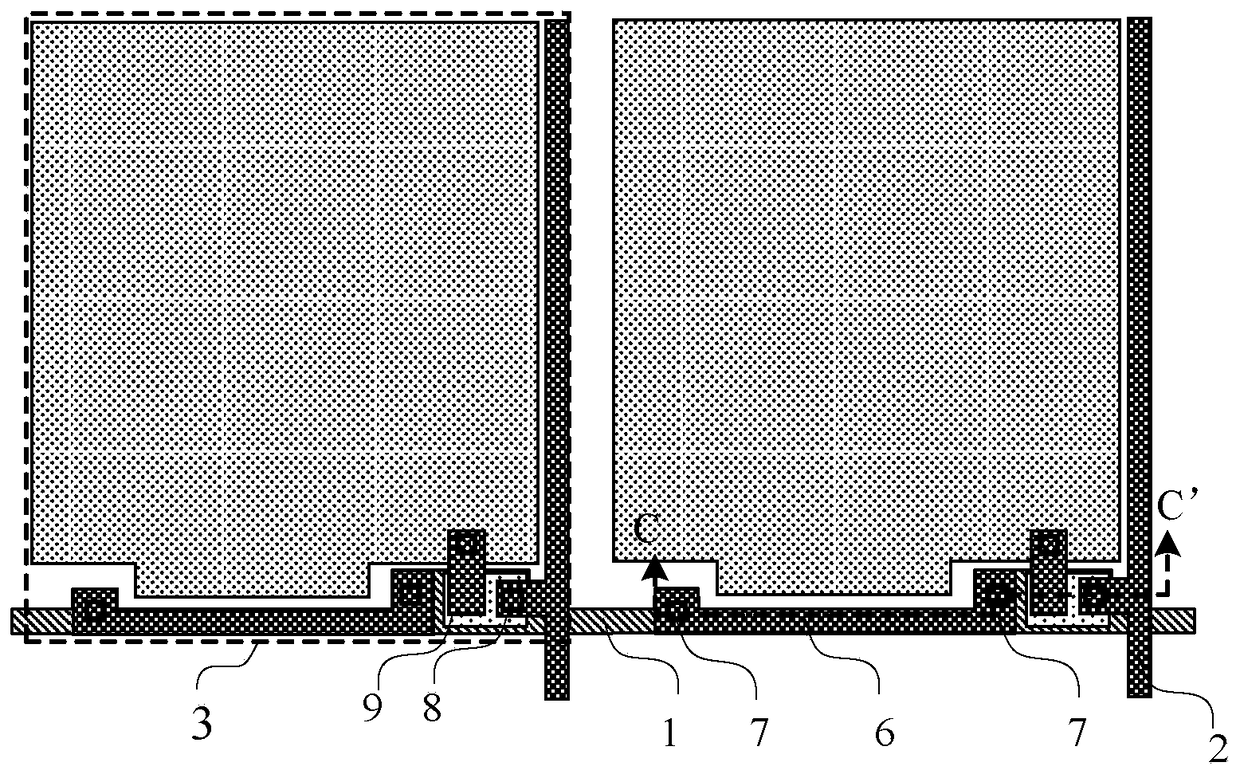
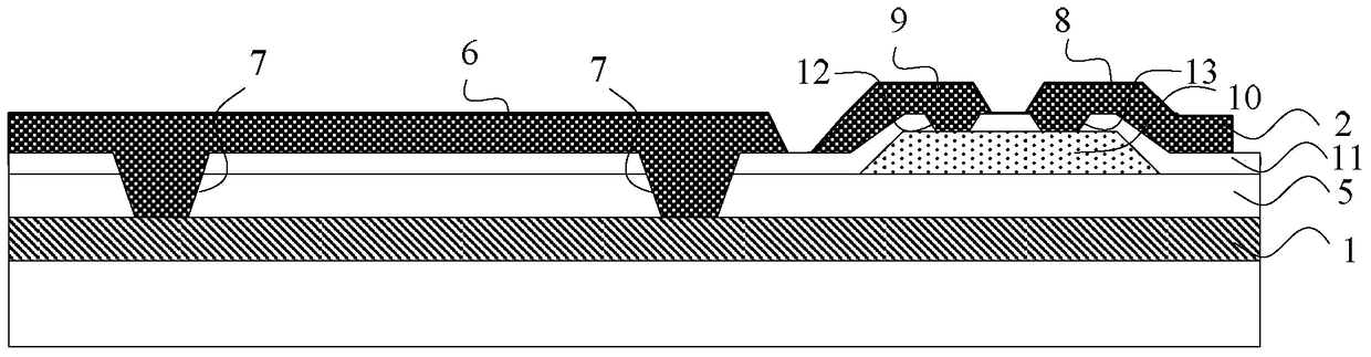
[0034] An embodiment of the present invention provides an array substrate, such as figure 2 and image 3 As shown, the array substrate includes a plurality of gate lines 1 parallel to each other, an insulating layer 5 located on the film layer where the plurality of gate lines 1 are located, and at least one first conductive structure 6 located on the insulating layer 5. The insulating layer 5 At least two first via holes 7 corresponding to the first conductive structure 6 are arranged on it, and the first conductive structure 6 is electrically connected to the gate line 1 through the first via holes 7 .

[0035] When the array substrate is in operation, since the first conductive structure 6 is electrically connected to the gate line 1 through at least two first via holes 7, the first conductive structure 6 is connected in parallel to the gate line 1, which is equivalent to connecting a resistor in parallel to the gate line 1. Therefore, the resistance value of the grid lin...

Embodiment 2

[0054] An embodiment of the present invention provides a method for manufacturing an array substrate, such as Figure 9 As shown, the method includes:

[0055]S901, forming a gate metal layer, and forming a pattern including a gate line through a patterning process. Exemplarily, a gate metal layer is formed by methods such as plasma-enhanced chemical vapor deposition, sputtering, or thermal evaporation, and a photoresist is coated on the gate metal layer. The gate metal layer of the photoresist forms a pattern including gate lines after exposure, development, etching and other steps.

[0056] S902, forming an insulating layer on the film layer where the gate line is located, and forming at least two first via holes corresponding to the first conductive structure on the insulating layer through a patterning process. Exemplarily, by plasma-enhanced chemical vapor deposition, sputtering or thermal evaporation and other methods, an insulating layer is formed on the film layer wh...


PUM


Abstract

An array substrate and a manufacturing method thereof, and a display device are provided. The array substrate includes a plurality of mutually parallel signal lines, an insulating layer located on a layer in which the plurality of signal lines is located and at least one first conductive structure located on the insulating layer. The insulating layer includes at least two first through holes corresponding to the first conductive structure, and the first conductive structure is electrically connected with the signal lines through the at least two first through holes.

Description

technical field [0001] The present invention relates to the field of display technology, in particular to an array substrate, a manufacturing method thereof, and a display device. Background technique [0002] Usually, such as figure 1 As shown, the array substrate of the display device includes a plurality of gate lines 1 parallel to each other and a plurality of data lines 2 parallel to each other. The gate lines 1 and data lines 2 enclose a plurality of pixel units 3. A thin film transistor 4 is arranged at the intersection of the thin film transistor 4, and by controlling the on and off of the thin film transistor 4, the pixel unit 3 corresponding to the thin film transistor 4 can be controlled to display a picture, and further the display device can be controlled to display a picture. [0003] In the prior art, such as figure 1 As shown, the process of making the pixel unit 3 at position A display a picture is: the driving signal of the gate line 1 reaches the pixel u...

Claims


Application Information

Patent Timeline
Patent Type & Authority Patents(China)
IPC IPC(8): H01L27/12H01L21/77
CPCH01L27/124H01L21/77H01L27/12H01L27/1248H01L27/1262H01L27/127
Inventor 江鹏周茂秀杨海鹏戴珂尹傛俊王章涛
Owner BOE TECH GRP CO LTD
Why Eureka
Try Eureka