Module with a built-in semiconductor and method for producing the same

a technology of built-in semiconductors and modules, which is applied in the association of printed circuit non-printed electric components, dielectric characteristics, radiation controlled devices, etc., can solve the problems of inferior connection between wiring layers, passive components cannot be disposed on the overrunning portion of sealing resin, and the inner via cannot be disposed at a place, etc., to achieve the effect of convenient filling with conductive resin

Inactive Publication Date: 2006-11-28
PANASONIC CORP
View PDF5 Cites 44 Cited by
  • Summary
  • Abstract
  • Description
  • Claims
  • Application Information

AI Technical Summary

Benefits of technology

[0006]The module with a built-in semiconductor of the above construction is produced by a method which includes mounting a semiconductor device on a wiring layer formed on a circuit board, stacking on the circuit board an electrically insulating substrate having inner vias, and heating and pressurizing so that the semiconductor device is buried in the electrically insulating substrate. This production method has an advantage that filling through holes for the inner vias can be easily filled with a conductive resin and that a process for forming the inner via can be selected from a wide range. However, when using this production method, the inner via cannot be disposed at a place where the sealing resin extends over the edge portion of the semiconductor device. This is because when the electrically insulating substrate is stacked, the inner via cannot pierce a portion of the sealing resin which overruns the semiconductor, without deformation. The deformation of the inner via causes inferior connection between the wiring layers. Further, a passive component cannot be disposed on the overrunning portion of the sealing resin. As described above, the overrunning sealing resin reduces an area where the inner vias and the passive components can be mounted. As a result, when it is necessary to dispose a predetermined number of inner vias and passive components each of which has a predetermined size, an area of the module with a built-in semiconductor should be large, which is adverse to the requirement of miniaturization of the electronic equipment.

Problems solved by technology

However, when using this production method, the inner via cannot be disposed at a place where the sealing resin extends over the edge portion of the semiconductor device.
The deformation of the inner via causes inferior connection between the wiring layers.
Further, a passive component cannot be disposed on the overrunning portion of the sealing resin.
As a result, when it is necessary to dispose a predetermined number of inner vias and passive components each of which has a predetermined size, an area of the module with a built-in semiconductor should be large, which is adverse to the requirement of miniaturization of the electronic equipment.
However, when the semiconductor device is incorporated, the device is fixed securely by being surrounded entirely by the electrically insulating core layer in the final module, and therefore there is no practical problem even if the sealing resin is not used.

Method used


Image

  • Module with a built-in semiconductor and method for producing the same
  • Module with a built-in semiconductor and method for producing the same
  • Module with a built-in semiconductor and method for producing the same

Examples


first embodiment

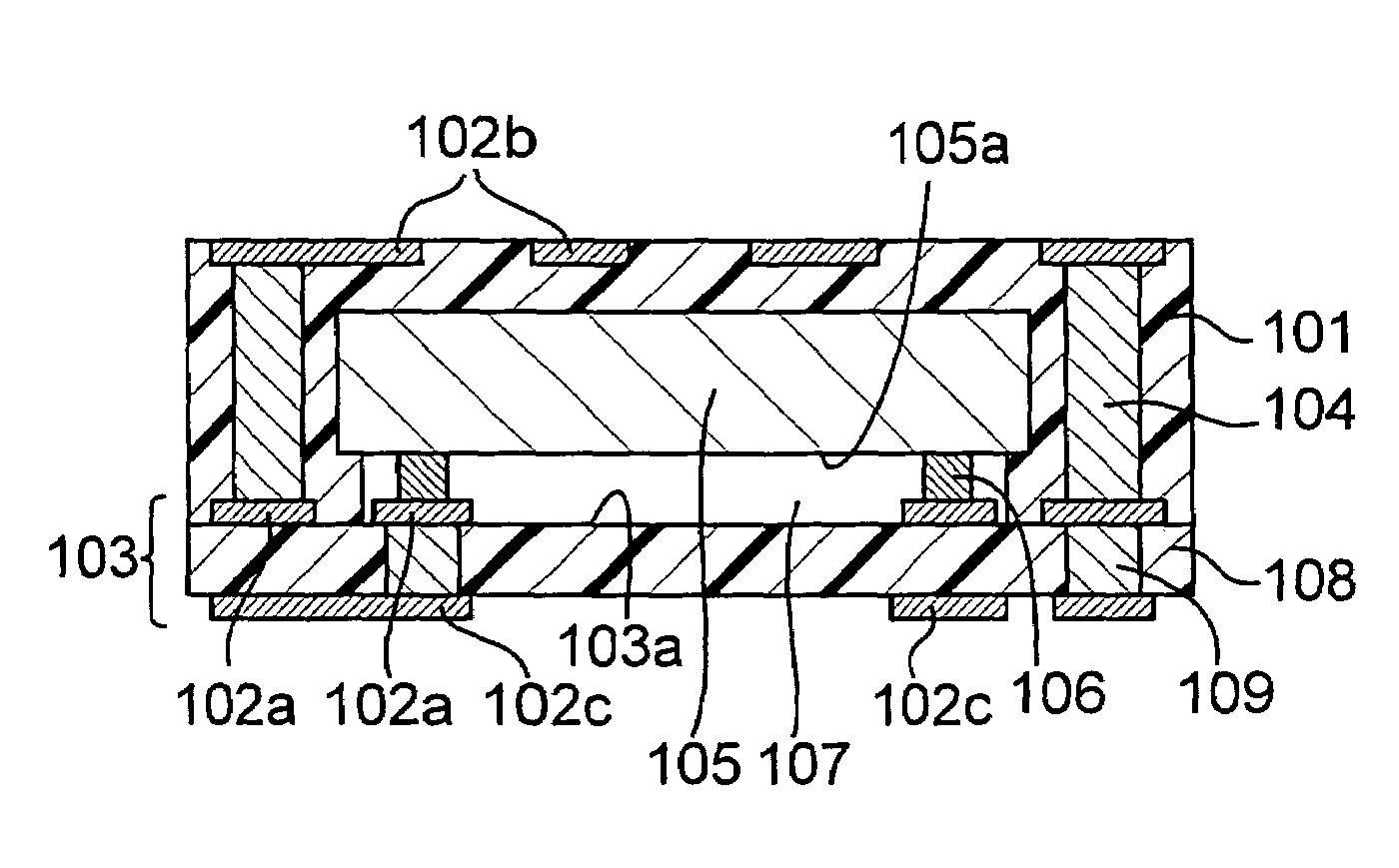
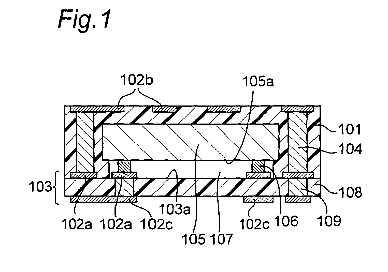
[0053]A first embodiment (Embodiment 1) of the present invention is described with reference to FIG. 1 which shows a cross-sectional view of a module with a built-in semiconductor. The module with a built-in semiconductor includes: an electrically insulating core layer 101, a first wiring layer 102a formed on one surface of the core layer 101 and a second wiring layer 102b formed on the other surface of the core layer, both of which have predetermined wiring patterns; a circuit board 103 having the first wiring layer 102a thereon, which closely adheres to the core layer; inner vias 104 electrically connecting the wiring layers 102a and 102b; and a semiconductor device 105 connected to the first wiring layer 102a and disposed within the core layer 101. The semiconductor device 105 is mounted by flip-chip bonding on the first wiring layer 102a, and the semiconductor device 105 and the first wiring layer 102a are electrically connected through protruding electrodes 106.

[0054]A space 10...

second embodiment

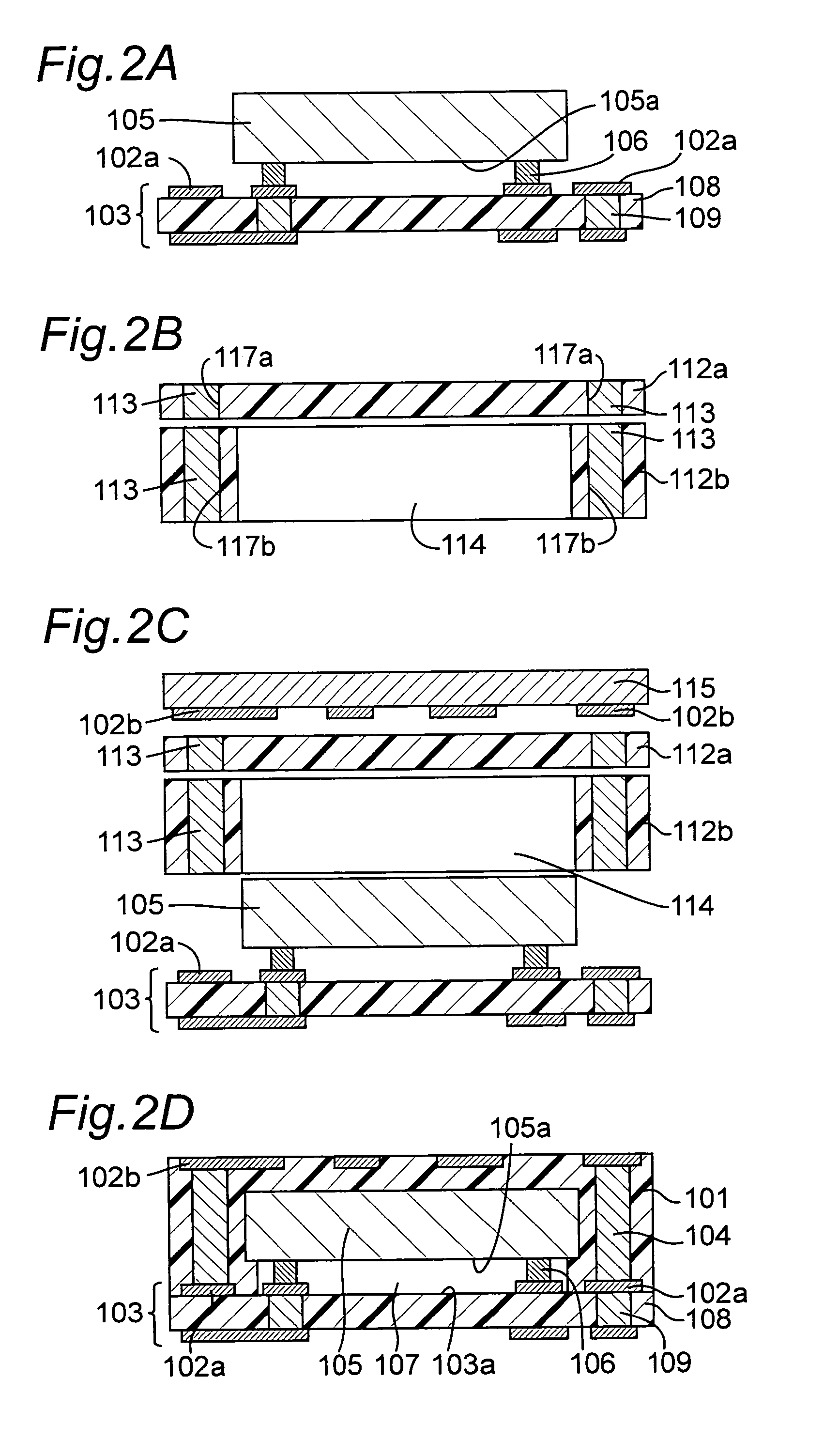
[0068]Next, as a second embodiment (Embodiment 2), a method for producing the module with a built-in semiconductor of Embodiment 1 is described. As described above, the production method of the present invention includes the steps of:

(1) mounting a semiconductor device on a wiring layer of a circuit board by flip-chip bonding;

(2) forming through bores in an electrically insulating substrate and filling the through bores with a conductive resin composition;

[0069](3) laminating the electrically insulating substrate on the circuit board with the mounted semiconductor device and laminating a mold release carrier having a wiring layer on a surface of the electrically insulating substrate which surface is opposite to the surface in contact with the circuit board; and

(4) fluidizing a thermosetting resin contained in the electrically insulating substrate and then curing the thermosetting resin and the conductive resin composition in the through bores by heating and pressurizing. These steps...

embodiment 3

[0087]A third embodiment (Embodiment 3) is described with reference to FIG. 3 which shows a cross-sectional view of a module with a built-in semiconductor device. The basic configuration (that is, the materials for the core layer 101, the connection between the first wiring layer 102a and the second wiring layer 102b with the inner vias 103, and the flip-chip bonding of the semiconductor device 105) of the module shown in FIG. 3 is similar to that of Embodiment 1. Therefore, differences from Embodiment 1 are described below.

[0088]The module shown in FIG. 3 is different from that shown in FIG. 1 in that the protruding electrodes 106 which connect the first wiring layer 102a and the semiconductor device 105 which is flip-chip bonded to the first wiring layer 102a is enclosed and sealed by the material of the core layer 101. This configuration provides an advantage that the connection reliability of the protruding electrodes 106 is increased since the protruding electrodes 106 are more...


PUM


Abstract

In a module with a built-in semiconductor, higher densification is achieved by disposing inner vias close to a semiconductor device. A module which has a space (107) between a first wiring layer (102a) and a built-in semiconductor device (105). The module is obtained by: mounting the semiconductor device (105) on a first wiring layer (102a) of a wiring board (103) without using a sealing resin; stacking on the circuit board an electrically insulating substrate having a through bore (inner via) (104) filled with a conductive paste and an opening for receiving the semiconductor device, and a mold release carrier having a second wiring layer (102b) in the stated order; and heating and pressurizing so that the semiconductor device (105) is incorporated in a core layer (101) which is formed by curing the electrically insulating substrate.

Description

CROSS-REFERENCE TO RELATED APPLICATIONS[0001]The present application claims a priority under 35 U.S.C. §119 to Japanese Patent Application No. 2003-190879 filed on Jul. 3, 2003, entitled “Module with a built-in semiconductor and method for producing the same.” The contents of that application are incorporated herein by the reference thereto in their entirety.FIELD OF THE INVENTION[0002]The present invention relates to a module with a built-in semiconductor wherein a semiconductor device is incorporated, and a method for producing the module.BACKGROUND OF THE INVENTION[0003]Recently, a higher density semiconductor with more functions is needed, since electronic equipment having higher performance and smaller size is required. For this reason, a three-dimensional mounting technique has been actively developed, wherein semiconductor devices and components are mounted three-dimensionally to reduce the mounting area. The three-dimensional mounting has the advantage of shortening a wire l...

Claims


Application Information

Patent Timeline
Patent Type & Authority Patents(United States)
IPC IPC(8): H01L29/40H01L23/31H01L23/538H01L27/146H01L27/148H01L31/0203H01L31/0232H05K1/18H05K3/20H05K3/46
CPCH01L23/3121H01L23/315H01L23/5385H01L27/14618H01L27/14643H01L31/0203H01L31/0232H05K1/186H01L27/148H01L2224/16225H01L2924/01046H01L2924/01078H01L2924/01079H01L2924/09701H01L2924/19041H05K1/0272H05K3/20H05K3/4614H05K2201/0108H05K2201/0209H05K2201/091H05K2201/10121H05K2201/10378H05K2201/10674H01L2924/19105H01L31/02325
Inventor KOJIMA, TOSHIYUKINAKATANI, SEIICHISUGAYA, YASUHIROYAMAMOTO, YOSHIYUKI
Owner PANASONIC CORP
Why Eureka
Try Eureka