Semiconductor probe with resistive tip and method of fabricating the same, and information recording apparatus, information reproducing apparatus, and information measuring apparatus having the semiconductor probe

a semiconductor probe and resistive tip technology, applied in the field of high-speed, sensitive semiconductor probes, can solve the problems of difficult to reduce the size of existing hard disks and high integration of flash memories, and difficult to make probes having a radius of several tens of nanometers into array forms

Inactive Publication Date: 2006-11-28
SAMSUNG ELECTRONICS CO LTD
View PDF16 Cites 15 Cited by
  • Summary
  • Abstract
  • Description
  • Claims
  • Application Information

AI Technical Summary

Problems solved by technology

It is not easy to reduce the size of existing hard disks and to highly integrate flash memories.
Thus, it is not easy to make probes having a radius of several tens of nanometers into an array form.
However, since the precision of a photolithographic process decreases considerably when a tip is formed to a height of several tens of nanometers, it is difficult to form a source area and a drain area so as to make a short channel.

Method used


Image

  • Semiconductor probe with resistive tip and method of fabricating the same, and information recording apparatus, information reproducing apparatus, and information measuring apparatus having the semiconductor probe
  • Semiconductor probe with resistive tip and method of fabricating the same, and information recording apparatus, information reproducing apparatus, and information measuring apparatus having the semiconductor probe
  • Semiconductor probe with resistive tip and method of fabricating the same, and information recording apparatus, information reproducing apparatus, and information measuring apparatus having the semiconductor probe

Examples


Embodiment Construction

[0039]Hereinafter, a semiconductor probe and a method of fabricating the same according to an embodiment of the present invention will be described in detail with reference to the attached drawings.

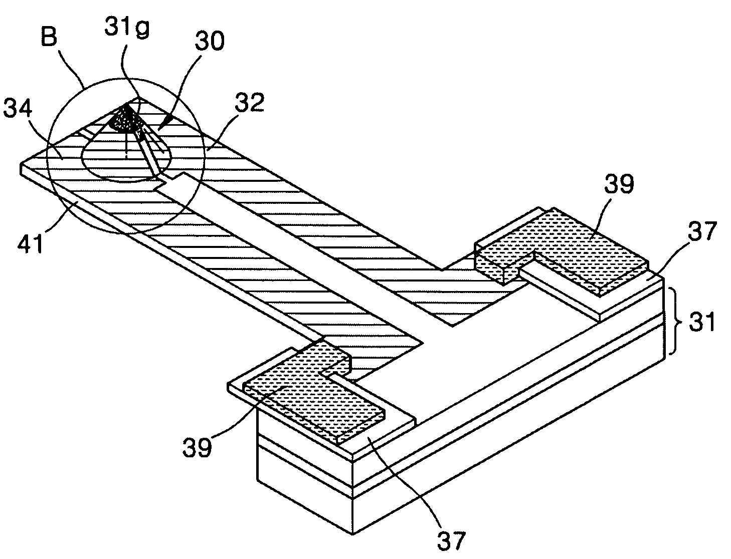
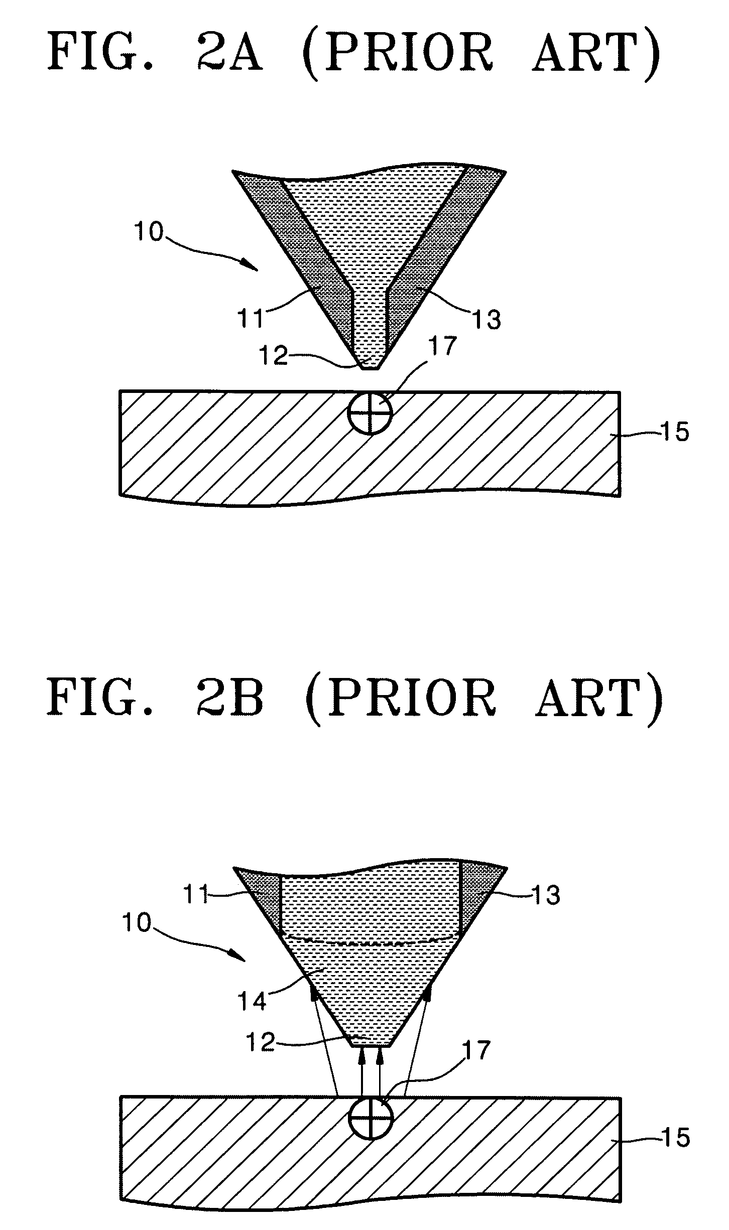
[0040]FIG. 3 is a schematic cross-sectional view illustrating a resistive tip of a semiconductor probe according to an embodiment of the present invention. Referring to FIG. 3, a resistive tip 50 includes a body 58 doped with first impurities, a resistive area 56, which is positioned at the peak of a resistive tip of the semiconductor probe 50 and lightly doped with second impurities, and first and second semiconductor electrode areas 52 and 54, which are formed on the slope around the resistive area 56 of the resistive tip 50 and are highly doped with the second impurities. Here, if the first impurities are p-type impurities, the second impurities are n-type impurities. If the first impurities are n-type impurities, the second impurities are p-type impurities.

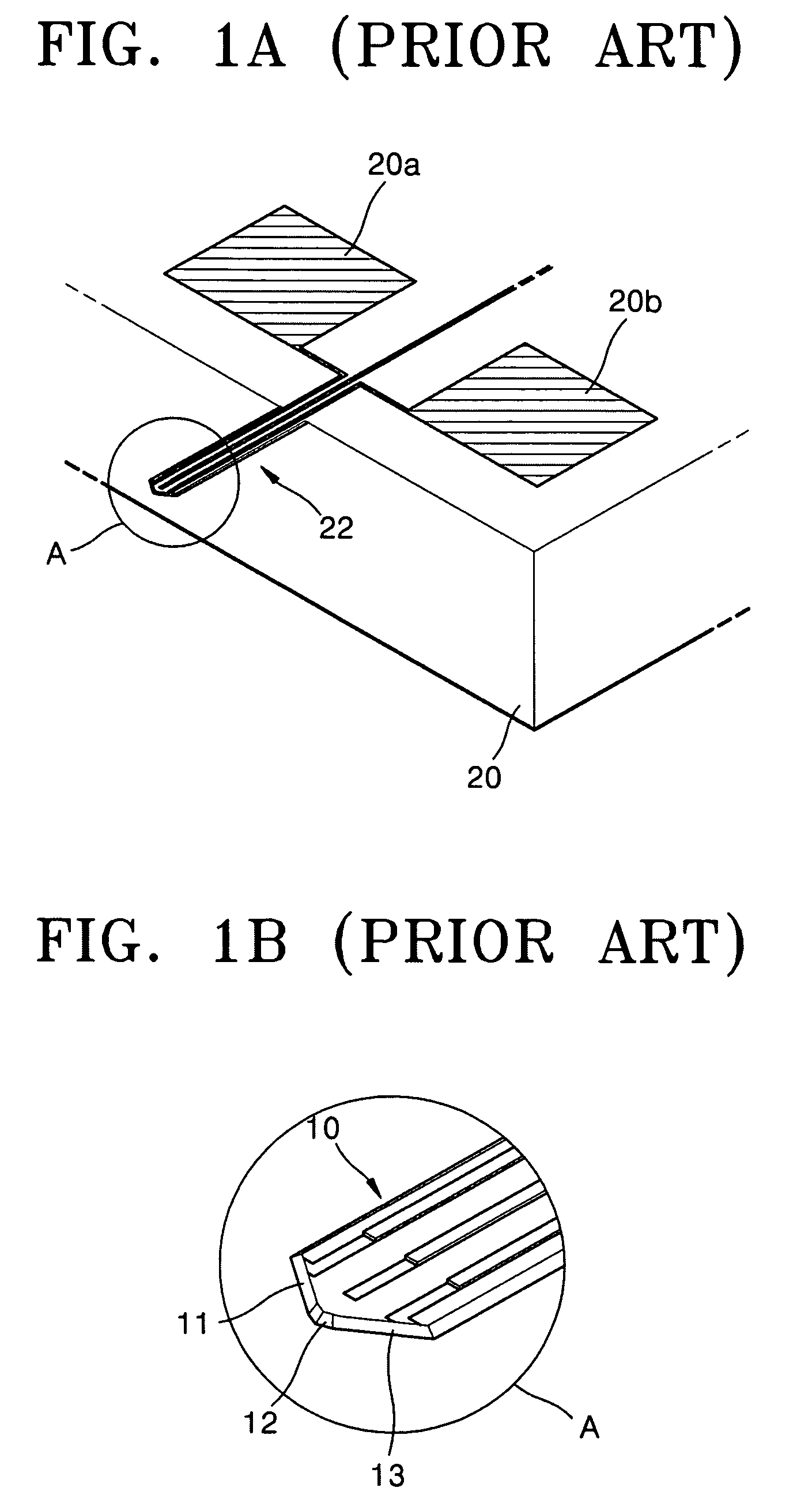
[0041]In the semiconductor p...


PUM

PropertyMeasurementUnit
ferroelectricaaaaaaaaaa
dielectric polarizationaaaaaaaaaa
semiconductoraaaaaaaaaa

Abstract

Provided are a semiconductor probe having a resistive tip, a method of fabricating the semiconductor probe, and a method of recording and reproducing information using the semiconductor probe. The semiconductor probe includes a tip and a cantilever. The tip is doped with first impurities. The cantilever has an end portion on which the tip is positioned. The tip includes a resistive area, and first and second semiconductor electrode areas. The resistive area is positioned at the peak of the tip and lightly doped with second impurities that are different from the first impurities. The first and second semiconductor electrode areas are heavily doped with the second impurities and contact the resistive area.

Description

BACKGROUND OF THE INVENTION[0001]This application claims the benefit of Korean Patent Application No. 2002-25400, filed on May 8, 2002, in the Korean Intellectual Property Office, the disclosure of which is incorporated herein in its entirety by reference.[0002]1. Field of the Invention[0003]The present invention relates to a high-speed, sensitive semiconductor probe with a resistive tip and a method of fabricating the same, and to an information recording apparatus, an information reproducing apparatus, and an information measuring apparatus having the semiconductor probe.[0004]2. Description of the Related Art[0005]As the demand for small-sized products such as portable communication terminals and electronic notes increases, highly-integrated micro nonvolatile recording media are increasingly required. It is not easy to reduce the size of existing hard disks and to highly integrate flash memories. Thus, information storage media and method using a scanning probe have been studied ...

Claims


Application Information

Patent Timeline
Patent Type & Authority Patents(United States)
IPC IPC(8): G01R31/02G01Q60/48G01Q70/16G11B9/14G11B9/00G11B9/02G11B11/08H01L21/66
CPCB82Y10/00B82Y35/00G11B9/02G11B9/14G11B9/1409G11B9/1418G01Q60/40G11B11/08H01L22/00
Inventor PARK, HONG-SIKSHIN, HYUN-JUNGJUNG, JU-HWAN
Owner SAMSUNG ELECTRONICS CO LTD
Why Eureka
Try Eureka