Edge bead removal inspection by reflectometry

a technology of reflectometry and bead removal, which is applied in the direction of optical radiation measurement, semiconductor/solid-state device testing/measurement, instruments, etc., can solve the problems of affecting the accuracy of optical diffraction, and affecting the accuracy of multi-layer structures, etc., to achieve accurate multi-layer structures and low cost

Active Publication Date: 2006-11-28
KLA TENCOR TECH CORP
View PDF2 Cites 26 Cited by
  • Summary
  • Abstract
  • Description
  • Claims
  • Application Information

AI Technical Summary

Benefits of technology

[0009]It is a further object of this invention to provide an improved integrated circuit manufacturing method and apparatus for edge bead removal inspection which is accurate for multilayer structures.
[0010]

Problems solved by technology

This edge bead can cause significant problems later in the process if not removed, including flaking which becomes a particulate and contaminant source.
However, this method is inaccurate due to the differing absorption spectra and color appearances of various resists.
In

Method used


Image

  • Edge bead removal inspection by reflectometry
  • Edge bead removal inspection by reflectometry
  • Edge bead removal inspection by reflectometry

Examples


first embodiment

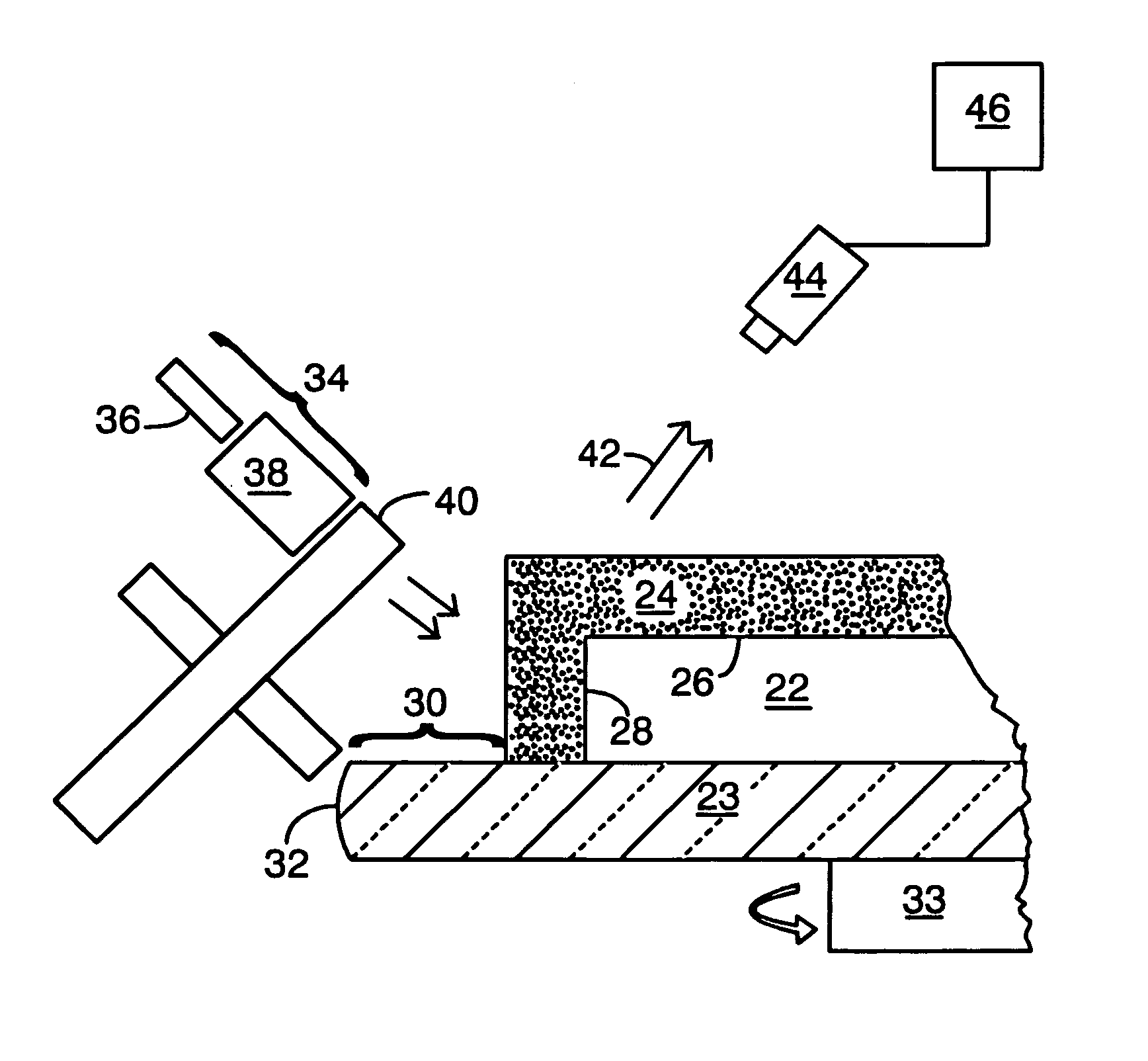
[0021]According to my inventive concept, a wafer is illuminated at the Brewster angle for silicon, and the reflected light image is observed in both s- and p-polarizations. In a first embodiment, the image acquired in p-polarization is subtracted from that acquired in s-polarization, yielding an “image difference”. Note that for the bare silicon region, there will be little or no p-polarized reflected light at the silicon Brewster angle, therefore the image difference will be essentially the same as the s-polarized image. In contrast, for the resist-covered region, the p-polarized light will be significantly reflected at the silicon Brewster angle, and the image difference will be significantly less bright than the s-polarized image. Sensitivity is maximized by using the image difference method. In this embodiment, identification of regions can be accomplished by thresholding the image differences, i.e, by assigning the characteristic that less than a certain difference is resist, a...

second embodiment

[0022]In a second embodiment, image differences are not created, but the p-polarized images are compared in the different regions, for light incident at a Brewster angle. For example, if the angle of incidence of the p-polarized light is the Brewster angle for silicon, the silicon regions will evidence little or no reflectance and will appear dark. In contrast, at that angle, there is significant reflectance from the resist-covered regions, which will appear considerably brighter than the silicon regions. Substantial contrast enhancement is thereby obtained using p-polarized light at the Brewster angle for silicon, as compared with the use of unpolarized light.

[0023]Both embodiments of this method therefore provide artificially enhanced image contrast between the bare silicon regions and the resist-covered regions. This enhanced contrast can help overcome the inherent noise present in the image near the wafer edge. It can also improve performance when multiple edge rings are present...


PUM


Abstract

A method and apparatus for enhancing image contrast between resist-covered and bare silicon regions of a wafer, applicable to Edge Bead Removal inspection. The wafer is illuminated separately by s-polarized light and p-polarized light impinging at near the Brewster angle of silicon or resist, and an image difference between the reflected s-polarized light and the reflected p-polarized light is derived.

Description

CROSS-REFERENCE TO RELATED APPLICATION[0001]This application corresponds to U.S. Provisional Application No. 60 / 467,996 filed May 5, 2003, and claims priority therefrom.FIELD OF THE INVENTION[0002]This invention relates to integrated circuit wafer inspection tools, and in particular to a method and apparatus for inspecting a wafer for removal of an edge bead of resist.BACKGROUND OF THE INVENTION[0003]During the manufacturing process for integrated circuits, lithography (which may include photolithography, e-beam lithography, or X-ray lithography) is generally utilized multiple times as part of patterning steps. The standard method of applying the resist used for lithography is a spin-on method, whereby resist is applied at or near the center of a rotating wafer, causing the resist to spread outwards across the wafer.[0004]The fluid dynamics of spin-coating result in the formation of an “edge bead” of resist, which is located at the wafer edge and is several times as thick as the dep...

Claims


Application Information

Patent Timeline
IPC IPC(8): G01J4/00G01N21/88G01N21/956G01N21/95H01L21/027H01L21/66
CPCG01N21/9503
Inventor ROSENGAUS, ELIEZER
Owner KLA TENCOR TECH CORP
Why Eureka
Try Eureka