On-chip system and method for measuring jitter tolerance of a clock and data recovery circuit

a clock and data recovery circuit technology, applied in the field of electronic circuitry testing, can solve the problems of many advanced integrated circuits operating too fast and becoming too complex to be tested only by external test equipmen

Inactive Publication Date: 2006-11-28
IBM CORP
View PDF9 Cites 72 Cited by
  • Summary
  • Abstract
  • Description
  • Claims
  • Application Information

AI Technical Summary

Benefits of technology

[0014]e) repeating steps c) and d) zero or more times to determine a maximum delayed clock phase for sampling the data stream, the maximum delayed clock phase representing a right timing signal margin.
[0015]Preferably, the on-chip method additionally ...

Problems solved by technology

Many advanced integrated circuits are operating too fast and are becoming too complex to be tested only by external test equipment.
However, as the BIST circui...

Method used


Image

  • On-chip system and method for measuring jitter tolerance of a clock and data recovery circuit
  • On-chip system and method for measuring jitter tolerance of a clock and data recovery circuit
  • On-chip system and method for measuring jitter tolerance of a clock and data recovery circuit

Examples


Embodiment Construction

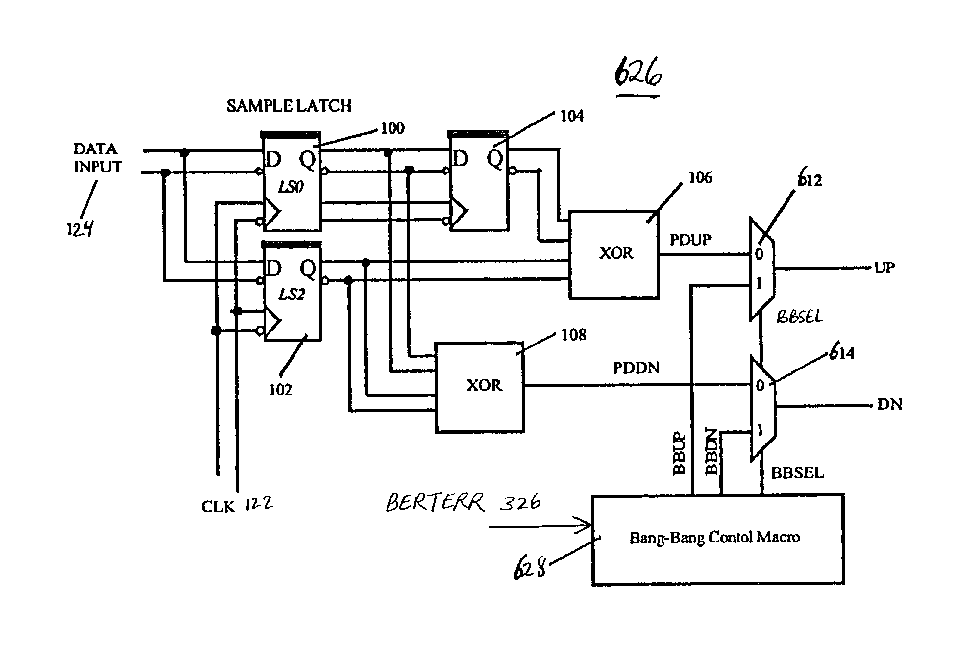
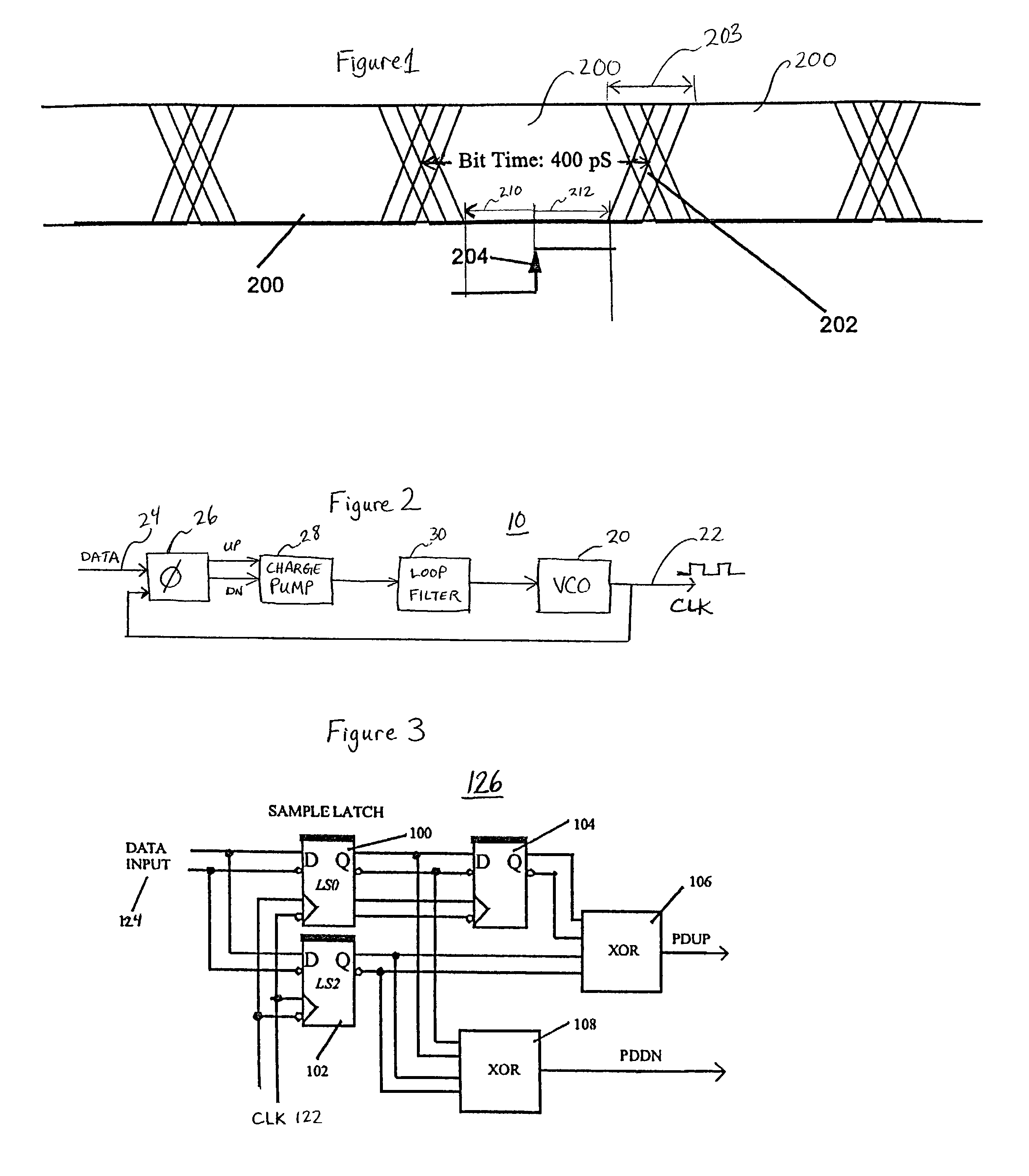
[0018]FIGS. 2 through 4 illustrate features of an on-chip system which is described as background to the present invention, but is not admitted to be prior art. FIG. 2 is a block diagram illustrating a clock recovery loop portion 10 of a clock and data recovery circuit (CDR), for use in recovering the clock phase of a data signal from a transmission line within an integrated circuit. The clock recovery loop is a phase lock loop (PLL) which includes a voltage controlled oscillator 20 which generates a clock signal 22 which is phase adjusted to sample the data signal 24 from the transmission line. To acquire and maintain phase lock, the generated clock signal 22 is provided as a feedback input, together with the data signal 24, to the bang-bang phase detector 26, which provides up and down phase control inputs to a charge pump 28. The charge pump 28, in turn, is coupled to a loop filter 30 which provides a control input to the VCO 20 to complete the clock recovery loop.

[0019]FIG. 3 is...


PUM


Abstract

An integrated circuit is operable to measure tolerance to jitter in a data stream signal. A Clock And Data Recovery Circuit (“CDR”) thereon recovers a phase of a clock for sampling a data stream signal containing a repeatable known sequence of data values and then samples the data stream signal with the recovered clock phase to obtain data stream sample data. An error rate determination circuit independently generates the repeatable known sequence of data values and compares them with the data stream sample data to determine an associated error rate. A control circuit coupled to the CDR delays the recovered clock phase by a predetermined amount a plurality of times and monitors the error rate after each time it delays the recovered clock phase. In this way, a maximum delayed clock phase is determined, representing a right timing signal margin for which the data stream signal can be sampled.

Description

FIELD OF THE INVENTION[0001]The present invention relates to testing of electronic circuitry and more specifically to an on-chip system and method for measuring the jitter tolerance of a clock and data recovery circuit.BACKGROUND OF THE INVENTION[0002]As integrated circuits increase in complexity, systems and methods must be capable of testing them to their limits, if the functionality under expected operating conditions is to be proven. Many advanced integrated circuits are operating too fast and are becoming too complex to be tested only by external test equipment. In place of external test equipment, more and more testing is being performed by circuitry implemented on the integrated circuit itself as built-in-self-test (BIST) circuitry. However, as the BIST circuitry becomes more complex, new systems and methods are needed to assure that integrated circuit functions are tested to the full limits they are required to operate.[0003]One type of data receiver used in integrated circu...

Claims


Application Information

Patent Timeline
IPC IPC(8): H03D3/24G01R31/317G01R31/3193
CPCG01R31/31709G01R31/31725G01R31/31937
Inventor SORNA, MICHAEL A.
Owner IBM CORP
Why Eureka
Try Eureka