Memory device having variable resistive memory element

a memory device and resistive memory technology, applied in the field of memory devices, can solve the problems of excessive resistance value of the combined resistance of the memory cell, and achieve the effects of high speed, fast writing, and preventing read-out errors

Active Publication Date: 2006-12-05
SONY CORP
View PDF3 Cites 33 Cited by
  • Summary
  • Abstract
  • Description
  • Claims
  • Application Information

AI Technical Summary

Benefits of technology

[0042]Moreover, when the information which has been recorded on the memory cell is read, the recorded information can be detected easily from an output signal based on the combined resistance value of the memory cell, and therefore a read-out error can be prevented from occurring.
[0044]Moreover, since the process of verification becomes unnecessary and also there is no need to apply repeatedly the voltage pulse, the writing can be performed quickly. Further, since the read-out error can be prevented from occurring, there is no need to perform the reading again. Accordingly, the recording of information or the read-out of information can be performed at a high speed.
[0045]According to the above mentioned present invention, the recording of information can be performed stably and the time required for recording of information can be shortened.
[0046]Accordingly, a memory device which can operate at a high speed and which has high reliability can be obtained.

Problems solved by technology

In other words, even when writing is further performed on the memory cell in which the writing has already been performed and the resistance value of the memory element has become low, there is no such case that the combined resistance value of the memory cell falls excessively.

Method used


Image

  • Memory device having variable resistive memory element
  • Memory device having variable resistive memory element
  • Memory device having variable resistive memory element

Examples


Embodiment Construction

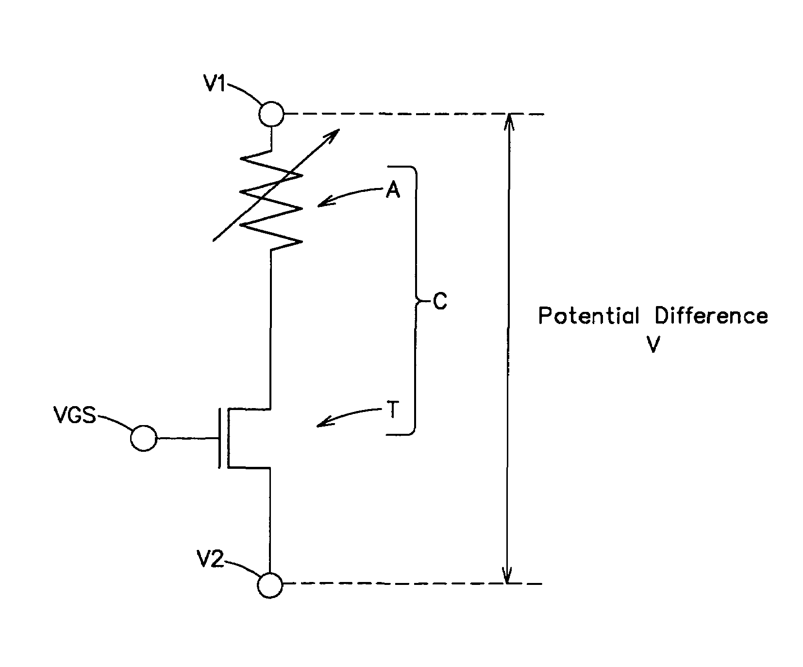
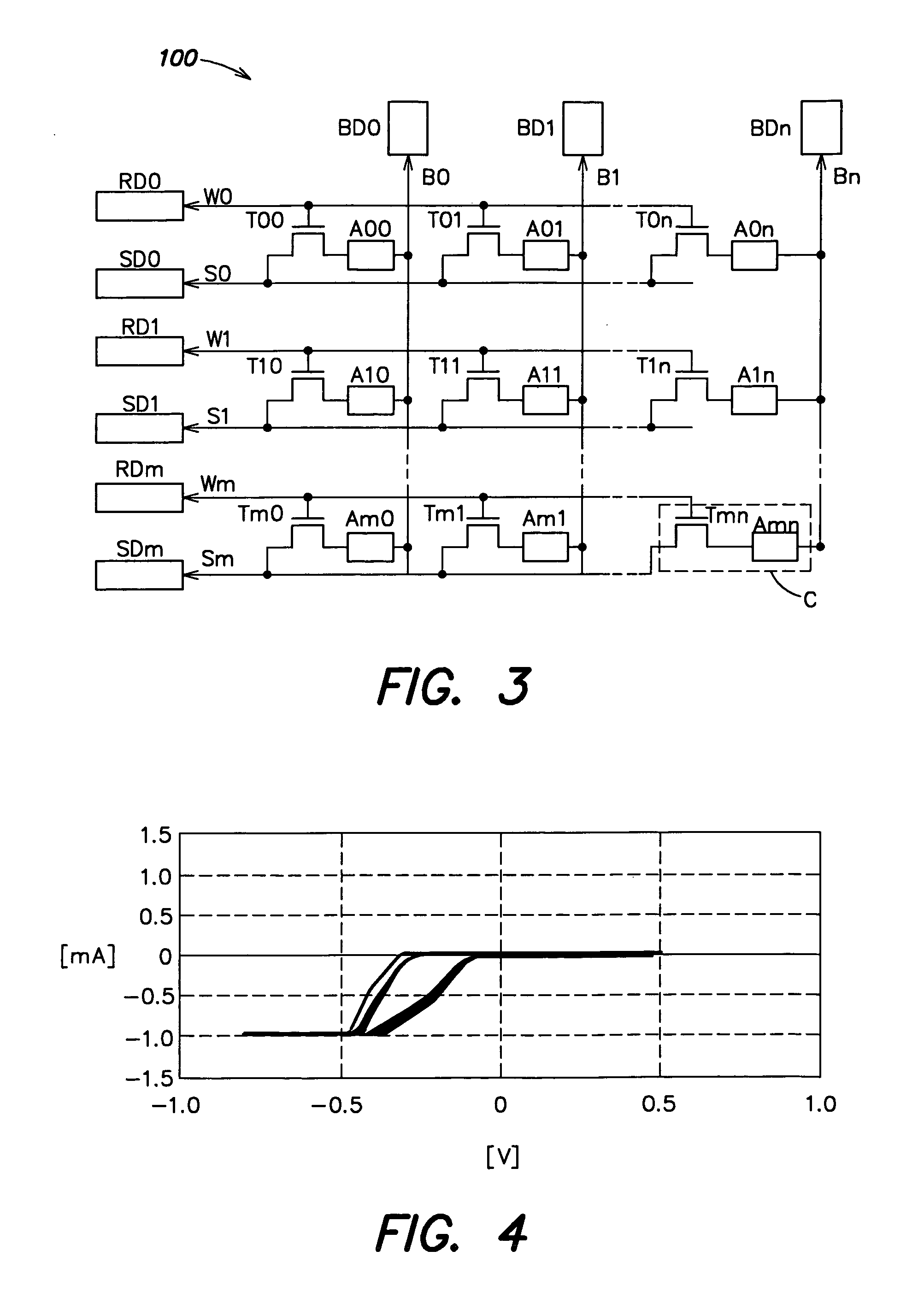
[0058]Hereinafter, an embodiment of a memory device according to the present invention is explained. In the present invention, the memory device includes a memory cell using a resistance change type memory element.

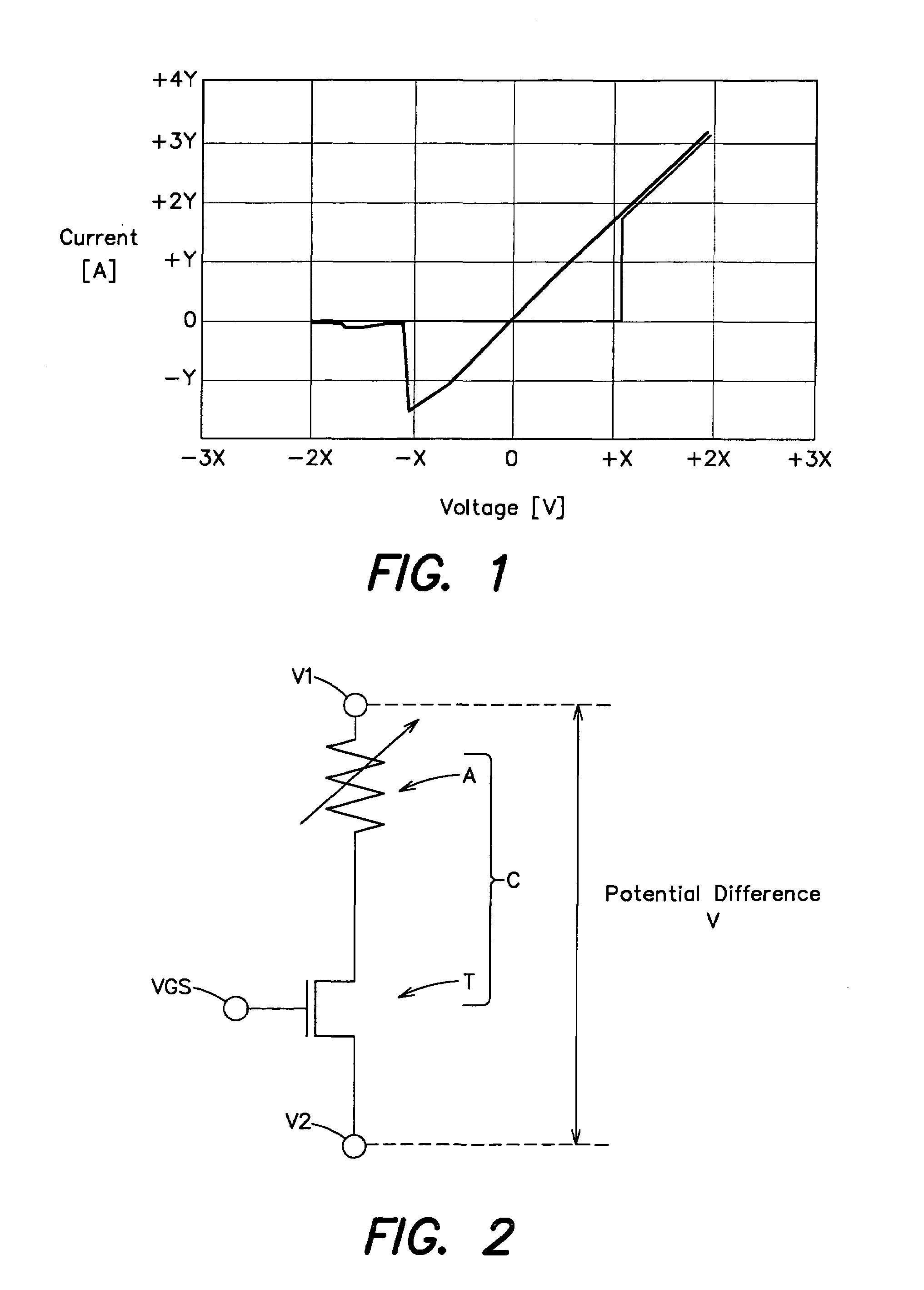
[0059]First, FIG. 1 shows the change of voltage and current of the resistance change type memory element used in a memory device in an embodiment of the memory device according to the present invention.

[0060]Specifically, in the initial state this resistance change type memory element is in a state where current can not flow easily, because a resistance value is large; however, when a voltage equal to or more than a writing threshold voltage (+1.1X [V] of FIG. 1, which is several hundreds milli-volts, for example) is applied, the current flows and the resistance value is lowered.

[0061]Then, the memory element changes into that having Ohmic characteristic, so that a state where the current flows in proportion to the voltage is obtained.

[0062]Subsequently, even if the voltag...


PUM


Abstract

A memory device is obtained in which stable recording of information can be performed and a period of time required for the recording of information can be shortened. The memory device includes a memory cell C formed of a memory element Amn having a characteristic in which a resistance value changes when applying between both ends of the memory element Amn a voltage equal to or more than a threshold voltage and a circuit element Tmn as a load connected in series to the memory element Amn; and when an operation to change the memory element Amn from a state of high resistance value to a state of low resistance value is defined as writing and when a voltage applied between both ends of the memory element Amn and the circuit element Tmn is equal to or more than a certain voltage value which is larger than the threshold voltage, the memory device has a characteristic in which a combined resistance value of the memory element Amn and the circuit element Tmn in the memory cell C after writing becomes almost constant value irrespective of the magnitude of applied voltage.

Description

BACKGROUND OF THE INVENTION[0001]1. Field of the Invention[0002]The present invention relates to a memory device in which a memory cell is formed using a memory element which stores information according to a state of electric resistance.[0003]2. Description of the Related Art[0004]In information equipment such as a computer, a high-density DRAM that performs a high-speed operation is widely used as a random access memory.[0005]However, since the DRAM is a volatile memory in which information disappears when a power supply is shut off, there has been a demand for a nonvolatile memory in which information does not disappear.[0006]Further, as the nonvolatile memory which is assumed to be promising in the future, there have been proposed an FeRAM (ferroelectric memory), an MRAM (magnetic memory), a phase change memory and a resistance change type memory such as a PMC (Programmable Metallization Cell) or an RRAM.[0007]In case of those memories, it becomes possible to retain written info...

Claims


Application Information

Patent Timeline
Patent Type & Authority Patents(United States)
IPC IPC(8): G11C11/00G11C13/00G11C8/00G11C13/02G11C16/02H01L21/8246H01L27/10H01L27/105H01L27/24H01L43/08H01L45/00
CPCG11C13/0009G11C13/0064G11C13/0069G11C13/0097H01L27/2436G11C13/0004G11C2013/009G11C2213/11G11C2213/15G11C2213/34G11C2213/79H01L45/085H01L45/1233H01L45/146H01L45/1625H10B63/30H10N70/245H10N70/826H10N70/8833H10N70/026G11C13/02G11C8/00
Inventor TSUSHIMA, TOMOHITOARATANI, KATSUHISAKOUCHIYAMA, AKIRA
Owner SONY CORP
Why Eureka
Try Eureka