Semiconductor integrated circuit device capable of controlling impedance

a technology of integrated circuit devices and semiconductors, applied in the field of can solve the problems of increasing the burden of designing semiconductor integrated circuit devices, enlarge the chip size and the number of pins,

Active Publication Date: 2006-12-12
SAMSUNG ELECTRONICS CO LTD
View PDF8 Cites 124 Cited by
  • Summary
  • Abstract
  • Description
  • Claims
  • Application Information

AI Technical Summary

Problems solved by technology

However, those techniques enlarge chip sizes and the number of pins to increase the burden of designing semiconductor integrated circuit devices.

Method used


Image

  • Semiconductor integrated circuit device capable of controlling impedance
  • Semiconductor integrated circuit device capable of controlling impedance
  • Semiconductor integrated circuit device capable of controlling impedance

Examples


Embodiment Construction

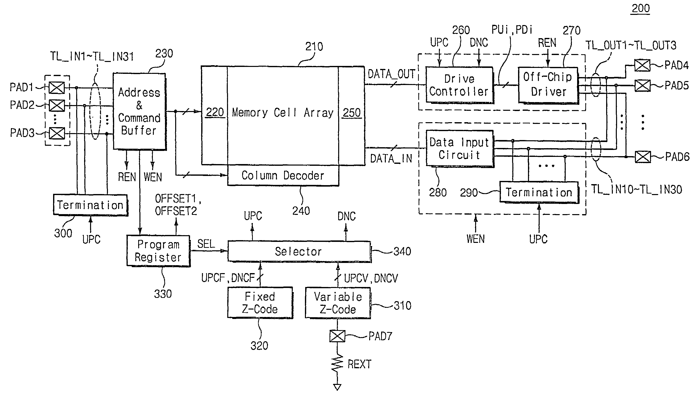
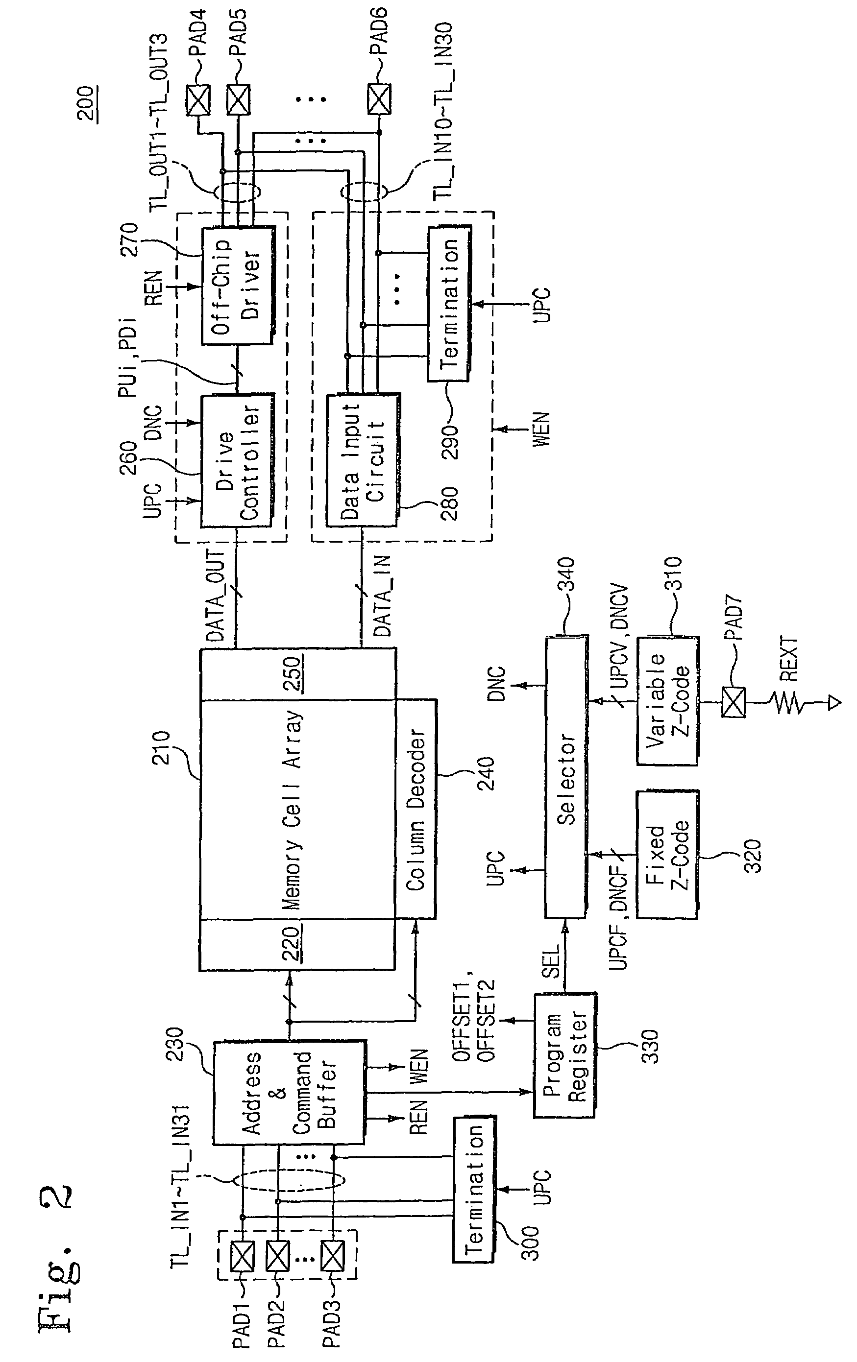
[0034]With reference now to the drawings wherein like or similar elements are designated with identical reference numerals throughout the several views and wherein various elements depicted are not necessarily drawn to scale.

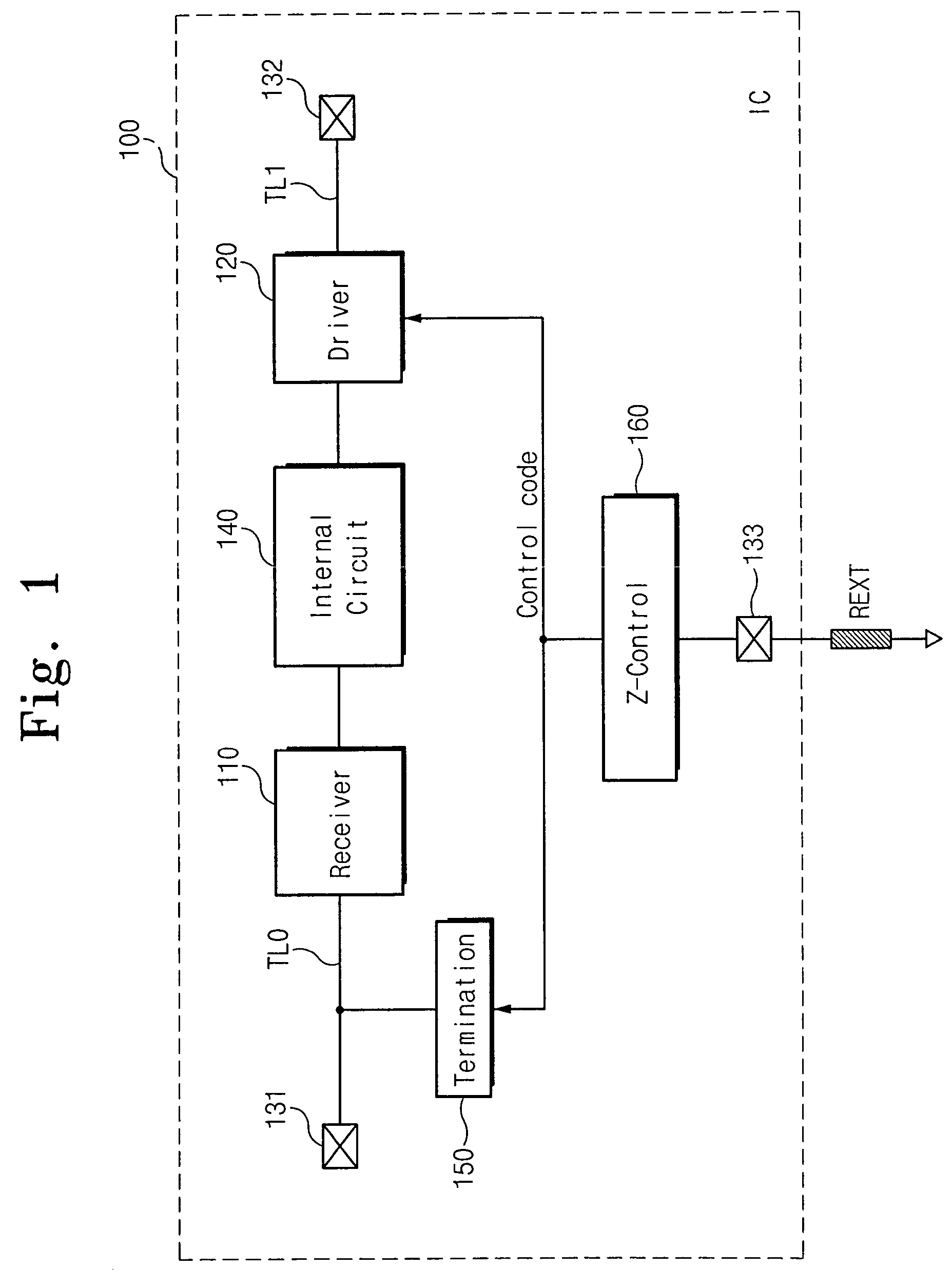
[0035]FIG. 1 is a block diagram of a semiconductor memory device according to the present invention. Referring to FIG. 1, the semiconductor integrated circuit device 100 is constructed to communicate other integrated circuit devices, including a receiver 110 and a driver 120. The receiver 110 is connected to a pad 131 through a signal transfer line TL0 to receive external signals (e.g., control signals or address signals) through the pad 131. The driver 120 is connected to a pad 132 through a signal transfer line TL1. The driver 120 operates the signal transfer line TL1 in response to internal signals (e.g., data signals).

[0036]To the signal transfer line TL0, a termination circuit 150 is connected. The pad 131 may be connected to other integrated circuit device...


PUM


Abstract

A semiconductor integrated circuit device is connected to an external reference resistor, including an impedance control circuit for generating impedance control codes variable with impedances established by the external reference resistor. An input circuit receives an external signal through an input transfer line and forwards the external signal to an internal circuit. A termination circuit terminates the input transfer line in response to at least one of the impedance control code. An output circuit drives an output transfer line in accordance with an output signal. Impedance is variable with the control codes.

Description

CROSS REFERENCE TO RELATED APPLICATIONS[0001]This application claims priority from Korean Patent Application No. 2003-57245, filed on Aug. 19, 2003, the contents of which are incorporated herein by reference in their entirety.BACKGROUND OF THE INVENTION[0002]1. Field of this Invention[0003]This disclosure relates to a semiconductor integrated circuit device, and more particularly, to a semiconductor integrated circuit device including circuits for programmable bus termination and impedance driving.[0004]2. Description of Related Art[0005]In designing high frequency integrated circuit devices associated with a double data rate (DDR) memory, it is becoming important with input / output AC characteristics of data, address, and control signals in accordance with the advancement of functionality in semiconductor device industries. The AC characteristics are more affected from the property of channels linking two or more numbers of devices, rather than from integrated circuit devices or con...

Claims


Application Information

Patent Timeline
Patent Type & Authority Patents(United States)
IPC IPC(8): H03K19/003H03K19/0175G11C7/00G11C11/401G11C11/409H03K19/00H04L25/02
CPCH03K19/0005H04L25/0278H04L25/028H04L25/0292G11C29/025G11C29/028G11C7/00
Inventor PARK, YOUN-SIK
Owner SAMSUNG ELECTRONICS CO LTD
Why Eureka
Try Eureka