Active protection circuit for load mismatched power amplifier

a protection circuit and power amplifier technology, applied in amplifier protection circuit arrangements, amplifiers with semiconductor devices/discharge tubes, amplifiers, etc., can solve the problems of excessive amplifier output power not reaching load, dispersed power damage or destroy transistors, and not all integrated circuit power transistors are capable of withstanding highly mismatched load impedances, so as to reduce the output power of the amplifier producing the overpeak voltage being detected

Inactive Publication Date: 2006-12-12
QORVO US INC
View PDF31 Cites 16 Cited by
  • Summary
  • Abstract
  • Description
  • Claims
  • Application Information

AI Technical Summary

Benefits of technology

[0007]A radio frequency (RF) amplifier driving a highly mismatched load impedance outputs an RF voltage that is over a predetermined level (overpeak voltage). A peak detector is used to detect the overpeak voltage. If an output overpeak voltage is detected, an emitter follower buffer is used to activate a clamping transistor. The clamping transistor is coupled to the output of a bias circuit, and the activated clamping transistor is used to limit a reference DC bias voltage output from the bias circuit. The reference DC voltage is applied to an RF amplifier—either the amplifier producing the RF output voltage being detected, or a previous amplifier in an amplifier chain that ends with the amplifier producing the RF output voltage being detected. The limited reference DC bias voltage limits the gain of the amplifier. Consequently, the output power of the amplifier producing the overpeak voltage being detected is reduced. Thus, the amplifier is protected when driving a highly mismatched load impedance.

Problems solved by technology

In load mismatch situations, excess amplifier output power fails to reach the load and must be dissipated by one or more power amplifier transistors in the amplifier.
In severe load mismatch conditions, this dissipated power damages or destroys the transistors.
However, not all integrated circuit power transistors are capable of withstanding highly mismatched load impedances.
The limited reference DC bias voltage limits the gain of the amplifier.

Method used


Image

  • Active protection circuit for load mismatched power amplifier
  • Active protection circuit for load mismatched power amplifier
  • Active protection circuit for load mismatched power amplifier

Examples


Embodiment Construction

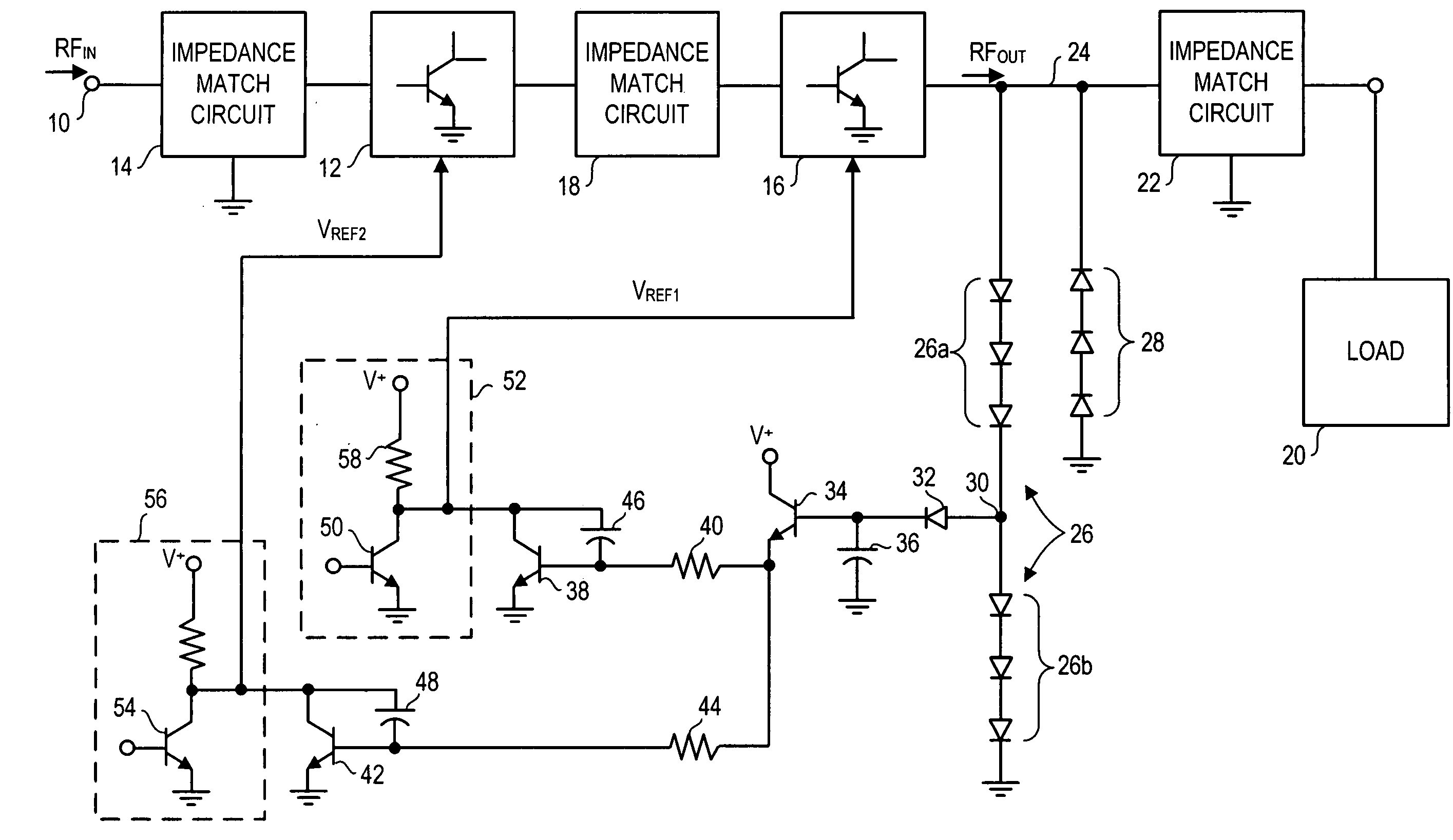
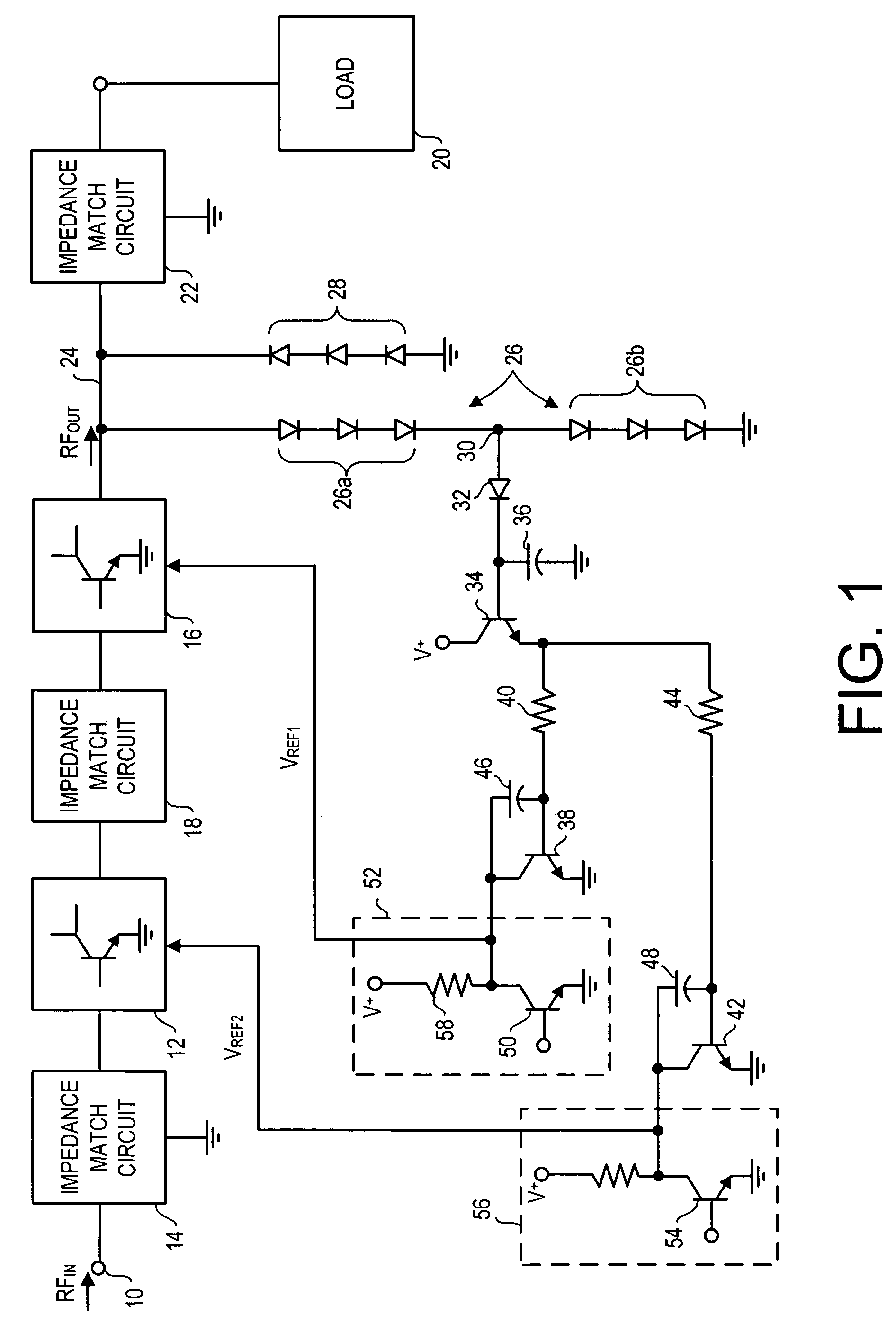
[0011]Skilled individuals will understand that certain known circuit elements are omitted from the accompanying drawing so as to more clearly illustrate the embodiment. Skilled individuals will also understand that electrical components such as resistors, capacitors, and diodes are selected due to the electrical properties they possess, and that various actual devices may provide the desired electrical properties. For example, in some embodiments the diodes are diode-connected bipolar transistors. The V+ symbol in the drawings illustrates a supply voltage and is not necessarily the same value at each indicated point.

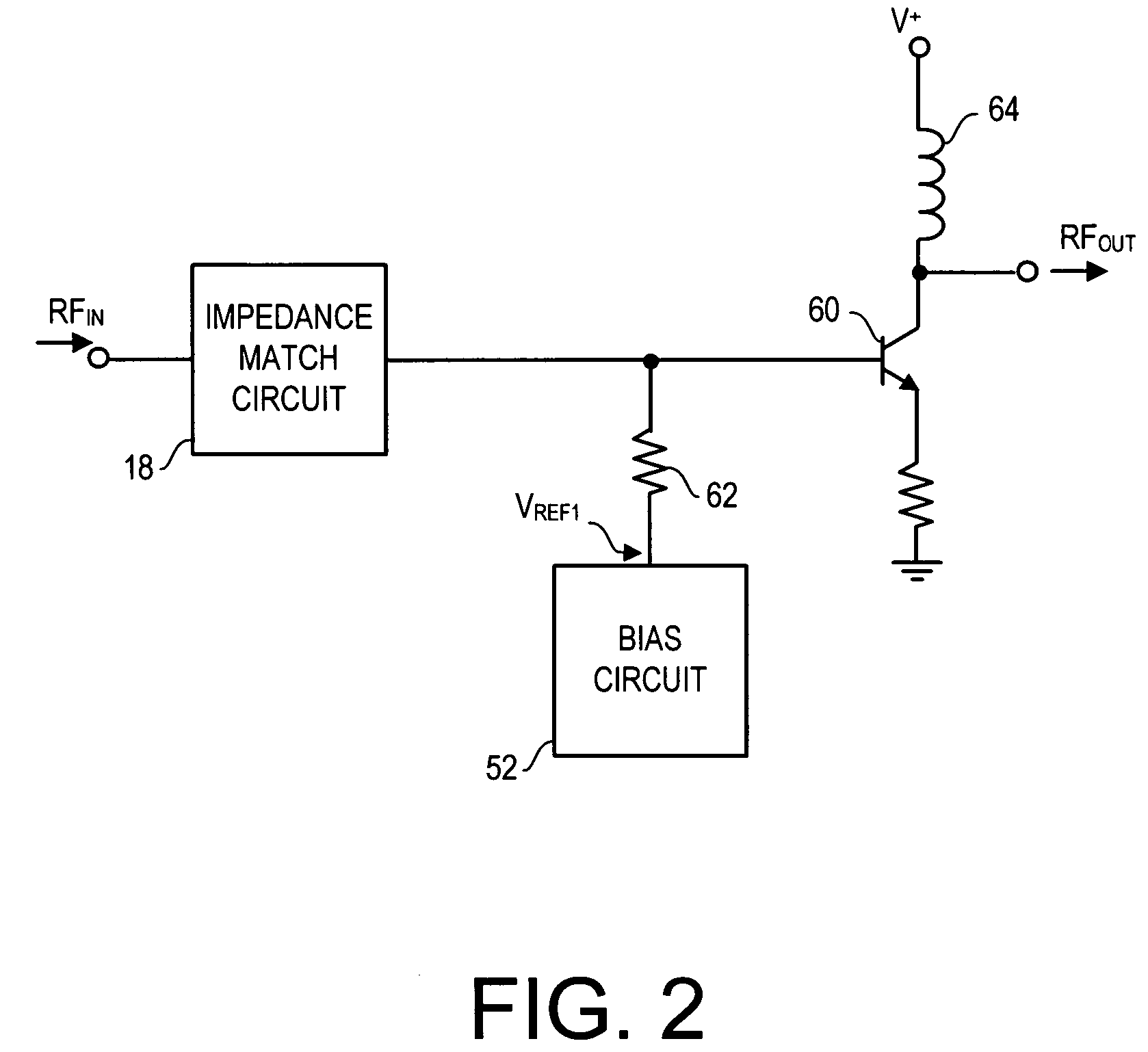
[0012]FIG. 1 is a combined diagrammatic and schematic view showing an embodiment of the invention. One embodiment is formed in a gallium arsenide (GaAs) integrated circuit. Other embodiments are formed in other semiconductor materials. As shown in FIG. 1, radio frequency (RF) input signal RFIN to be transmitted is received at input terminal 10 and is passed to RF driver ...


PUM


Abstract

A peak detector detects an amplifier output overvoltage condition if the amplifier drives a mismatched load impedance. In response to the detected overvoltage condition, a clamping transistor lowers a reference DC bias voltage supplied by a bias circuit to the amplifier. The lowered reference DC bias voltage lowers amplifier gain and output power, thus protecting the amplifier.

Description

CROSS-REFERENCE TO RELATED APPLICATION[0001]This application is a continuation of U.S. patent application Ser. No. 10 / 215,802, which was filed on Aug. 9, 2002, now U.S. Pat. No. 6,762,647 and is incorporated herein by reference in its entirety.BACKGROUND[0002]1. Field of Invention[0003]The invention is related to radio frequency (RF) power amplifier protection circuits.[0004]2. Description of the Related Art[0005]RF power amplifiers are intended to operate into a particular load impedance. This load impedance is typically set by an impedance matching circuit coupled to an antenna (load) used to radiate the amplified RF signal. In mobile transmitters (e.g., a cellular telephone handset), the proximity of the antenna to nearby objects (e.g., metal shopping carts) changes the load impedance.[0006]In load mismatch situations, excess amplifier output power fails to reach the load and must be dissipated by one or more power amplifier transistors in the amplifier. In severe load mismatch c...

Claims


Application Information

Patent Timeline
Patent Type & Authority Patents(United States)
IPC IPC(8): H03G3/10H03G3/30
CPCH03F1/52H03G3/3042
Inventor APEL, THOMAS R.
Owner QORVO US INC
Why Eureka
Try Eureka