
Semiconductor memory device and internal voltage generating method thereof

a memory device and semiconductor technology, applied in the field of semiconductor memory devices, can solve the problems of affecting and consuming power as much, and achieve the effect of maintaining the quality of internal power voltage and reducing power consumption

Active Publication Date: 2006-12-12
SK HYNIX INC
View PDF14 Cites 8 Cited by
  • Summary
  • Abstract
  • Description
  • Claims
  • Application Information

AI Technical Summary

Benefits of technology

This approach effectively reduces power consumption by maintaining internal power voltage quality and ensuring sufficient core voltage generation during precharge, preventing instability from insufficient core voltage supply.

Problems solved by technology

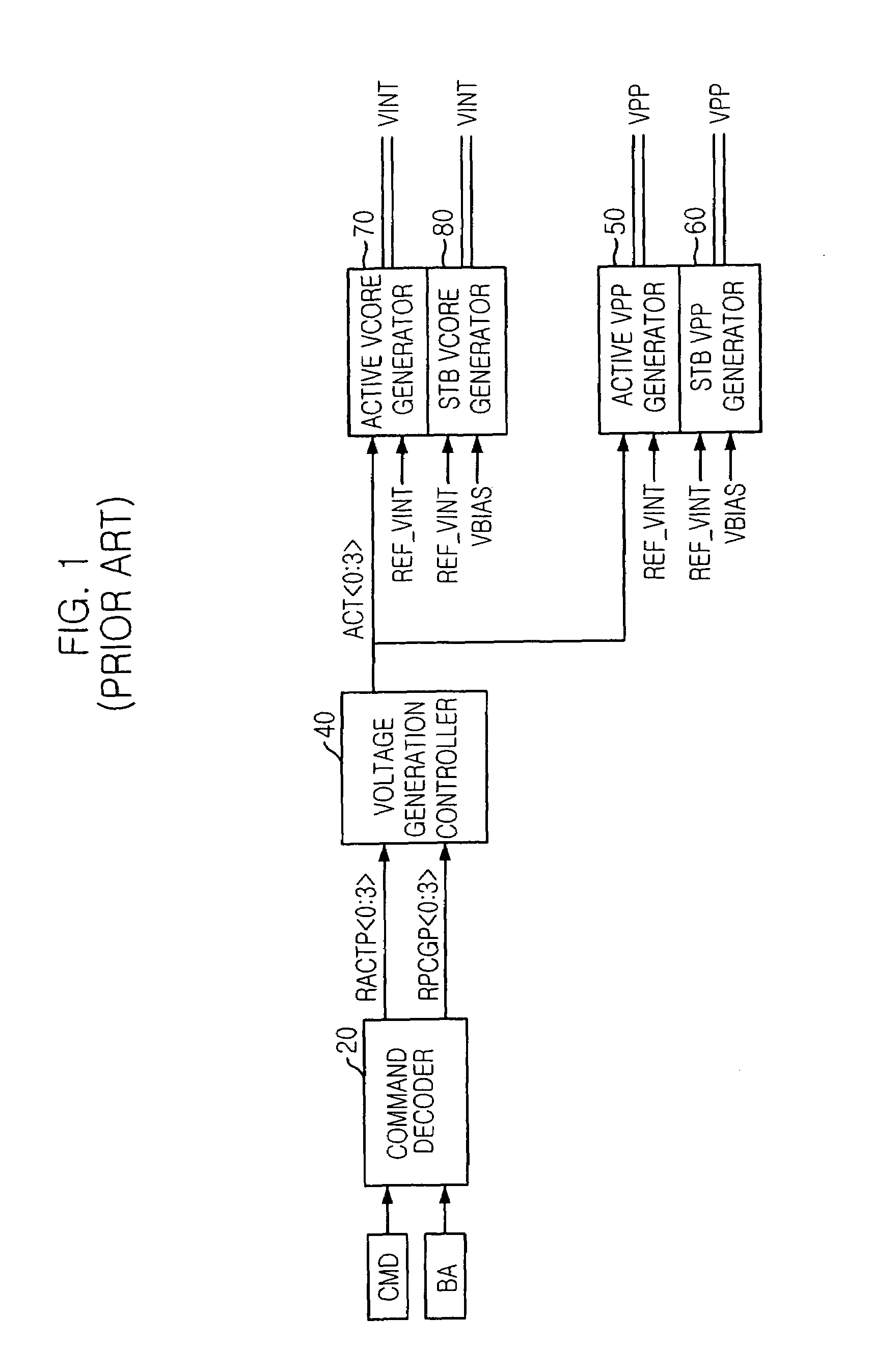
However, cell capacitor charge is a frequent operation, which is a basic operation of the memory device and, therefore, a charge voltage generating unit for supplying the core voltage VCORE consumes power as much as the internal power voltage generating unit.
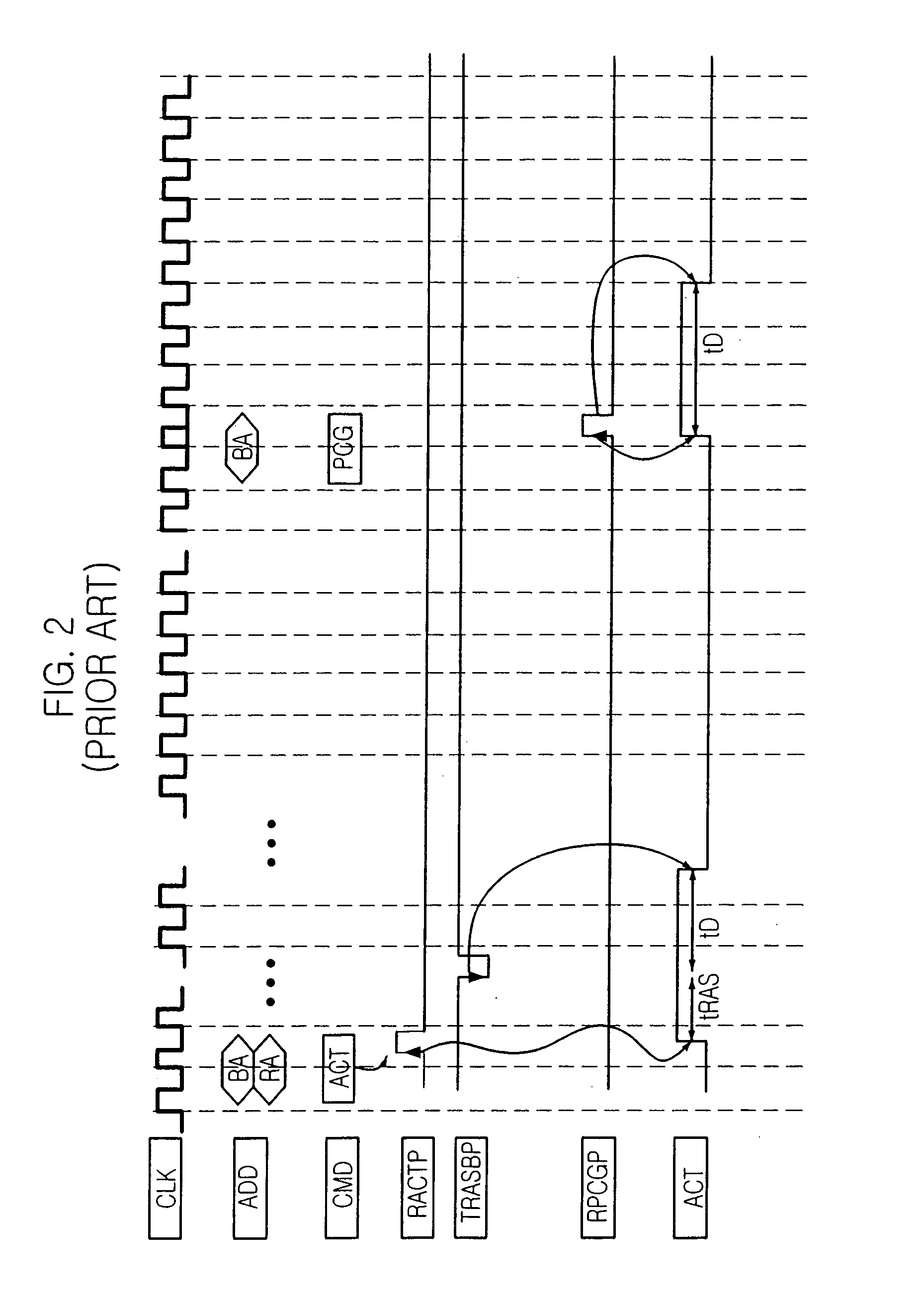
First, since the internal power voltage generating unit for raising the external power voltage has its own voltage detector for checking condition for raising the voltage, it is not necessary to turn off the device during the driven row active pulse and row precharge pulse. The quality of the internal power voltage can be deteriorated when the device is turned off as such.
Second, it is required more time to supply the core voltage than the internal power voltage in the precharge. Therefore, in the conventional technique in which the internal power voltage generating unit and the core voltage generating unit are controlled with one signal, the internal power voltage can be generated for too long time while the core voltage can be generated for too short time.

Method used


Image

  • Semiconductor memory device and internal voltage generating method thereof
  • Semiconductor memory device and internal voltage generating method thereof
  • Semiconductor memory device and internal voltage generating method thereof

Examples


Embodiment Construction

[0032]Hereinafter, a semiconductor memory device including an internal voltage generating circuit in accordance with the present invention will be described in detail referring to the accompanying drawings.

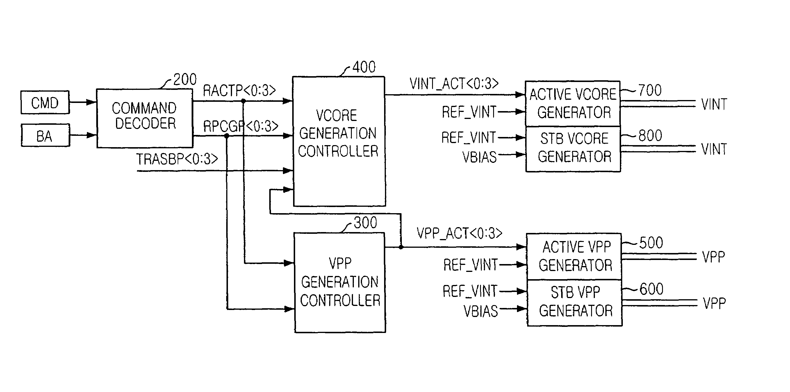
[0033]Referring to FIG. 3, a semiconductor memory device in accordance with an embodiment of the present invention includes a command decoder 200 receiving external control signals to output a row active signal RACTP and a row precharge signal RPCGP, an internal power voltage generation controlling unit 300 receiving the row active signal RACTP and the row precharge signal RPCGP for activating an internal power voltage active signal VPP_ACT for a predetermined time, a core voltage generation controlling unit 400 receiving the row active signal RACTP, the row precharge signal RPCGP and the internal power voltage active signal VPP_ACT for activating a core voltage active signal VINT_ACT for a predetermined time, an internal power voltage generating unit 500 for generating an interna...


PUM


Abstract

A semiconductor memory device reduces power consumption with maintaining quality of an internal power voltage and a core voltage. The semiconductor memory device reduces power consumption with sufficiently maintaining a core voltage during precharge. The semiconductor memory device includes a command decoder receiving external control signals to output an active signal and a precharge signal, an internal power voltage generation controlling unit receiving the active signal and the precharge signal for activating an internal power voltage active signal for a predetermined time, a core voltage generation controlling unit receiving the active signal, the precharge signal and the internal power voltage active signal for activating a core voltage active signal for a predetermined time, an internal power voltage generating unit for generating an internal power voltage during the activation period of the internal power voltage active signal; and a core voltage generating unit for generating a core voltage during the activation period of the core voltage active signal.

Description

FIELD OF INVENTION[0001]The present invention relates to a semiconductor memory device; and, more particularly, to a semiconductor memory device including an internal voltage generating circuit for reducing power consumption and an internal voltage generating method.DESCRIPTION OF PRIOR ART[0002]A semiconductor memory device includes circuit blocks for performing respective functions, to which a predetermined level of an internal power voltage is supplied as a driving voltage of each of the circuit blocks depending on requirement such as reference potential supply.[0003]Initially, an external power supply voltage VDD that is inputted to the device is directly used as the driving voltage. Recently, in the trend of low voltage environment, another approach is widely used, in which an internal power voltage VPP is generated by raising the level of the external power supply voltage VDD and the respective circuit blocks in the device are provided with the internal power voltage VPP.[0004...

Claims


Application Information

Patent Timeline
Patent Type & Authority Patents(United States)
IPC IPC(8): G11C5/14G11C11/4074G11C11/4076
CPCG11C5/147G11C11/4074G11C5/14
Inventor CHOI, JUN-GIKIM, YONG-KYU
Owner SK HYNIX INC
Learn More