Method for manufacturing wafer level chip stack package

a technology of chip stack and manufacturing method, which is applied in the direction of electrical apparatus, semiconductor device details, semiconductor/solid-state device devices, etc., can solve the problems of increasing the likelihood of reliability faults in the chip stack package, reducing mechanical strength, and forming space or voids between the two, so as to improve the mechanical strength and reliability of the resulting package

Active Publication Date: 2006-12-19
SAMSUNG ELECTRONICS CO LTD
View PDF8 Cites 351 Cited by
  • Summary
  • Abstract
  • Description
  • Claims
  • Application Information

AI Technical Summary

Benefits of technology

[0017]An exemplary embodiment of the present invention is directed to a method for manufacturing a WLCSP which may improve the mechanical strength and reliability of the resulting package.

Problems solved by technology

Although the semiconductor chips in the chip stack are physically and electrically connected, the formation of such a stack using only bump bonding tends to result in a space or void being formed between the opposing surfaces of two adjacent semiconductor chips.
Such spaces may cause reduced mechanical strength and increase the likelihood of reliability faults in the chip stack package.
However, because the liquid adhesive 123 used to fill the spaces between the adjacent semiconductor chips 111 typically includes metallic and / or non-metallic particulate filler materials, its flow characteristics may make it difficult to fill the space(s) between adjacent semiconductor chips completely or consistently, particularly for chip stacks having relatively small chip-to-chip spacing.
However, the adhesive tape may result in uneven pressure being applied to one or more of the semiconductor chips during a chip stacking process that may result in warpage of one or more of the semiconductor chips.

Method used


Image

  • Method for manufacturing wafer level chip stack package
  • Method for manufacturing wafer level chip stack package
  • Method for manufacturing wafer level chip stack package

Examples


Embodiment Construction

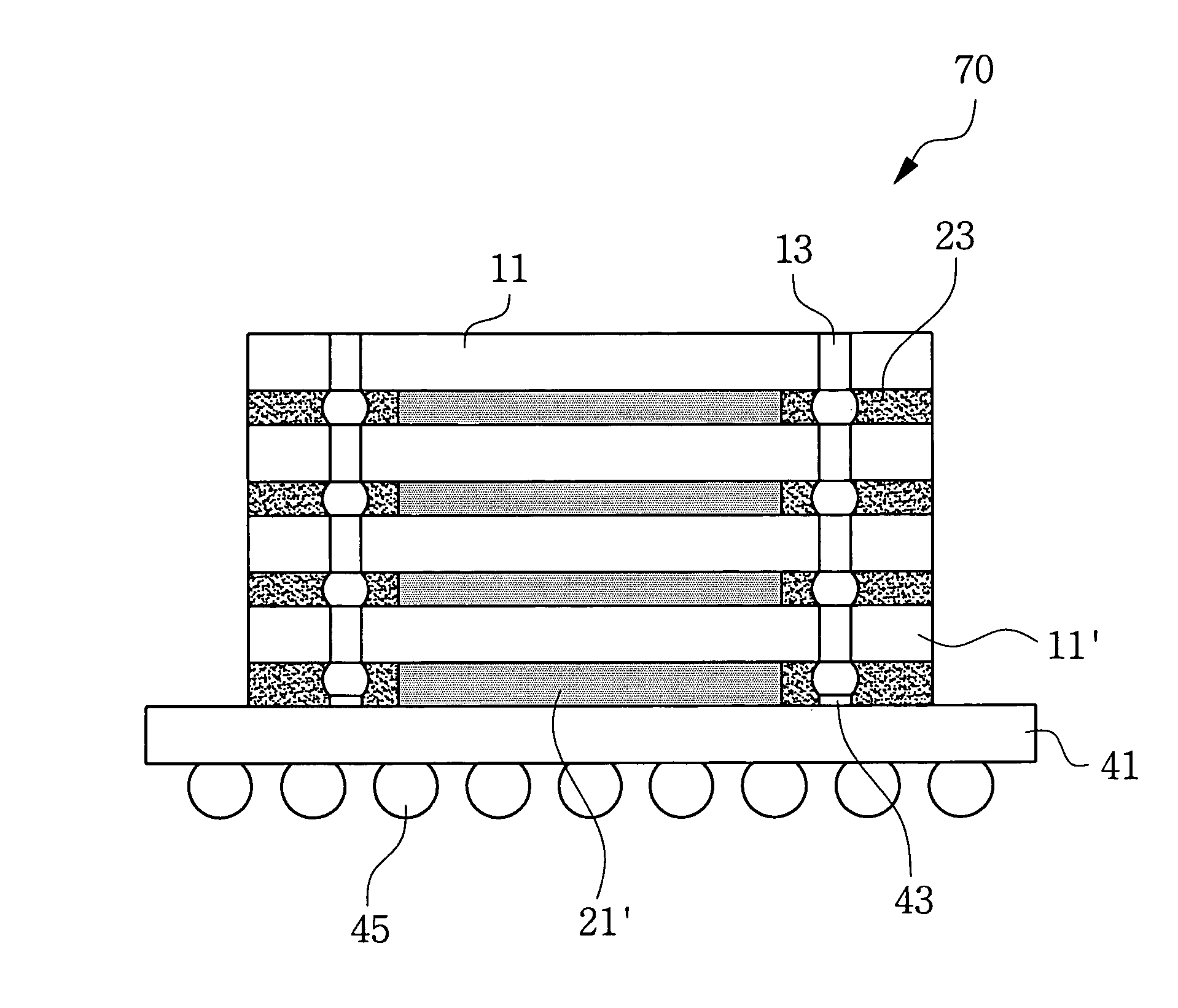
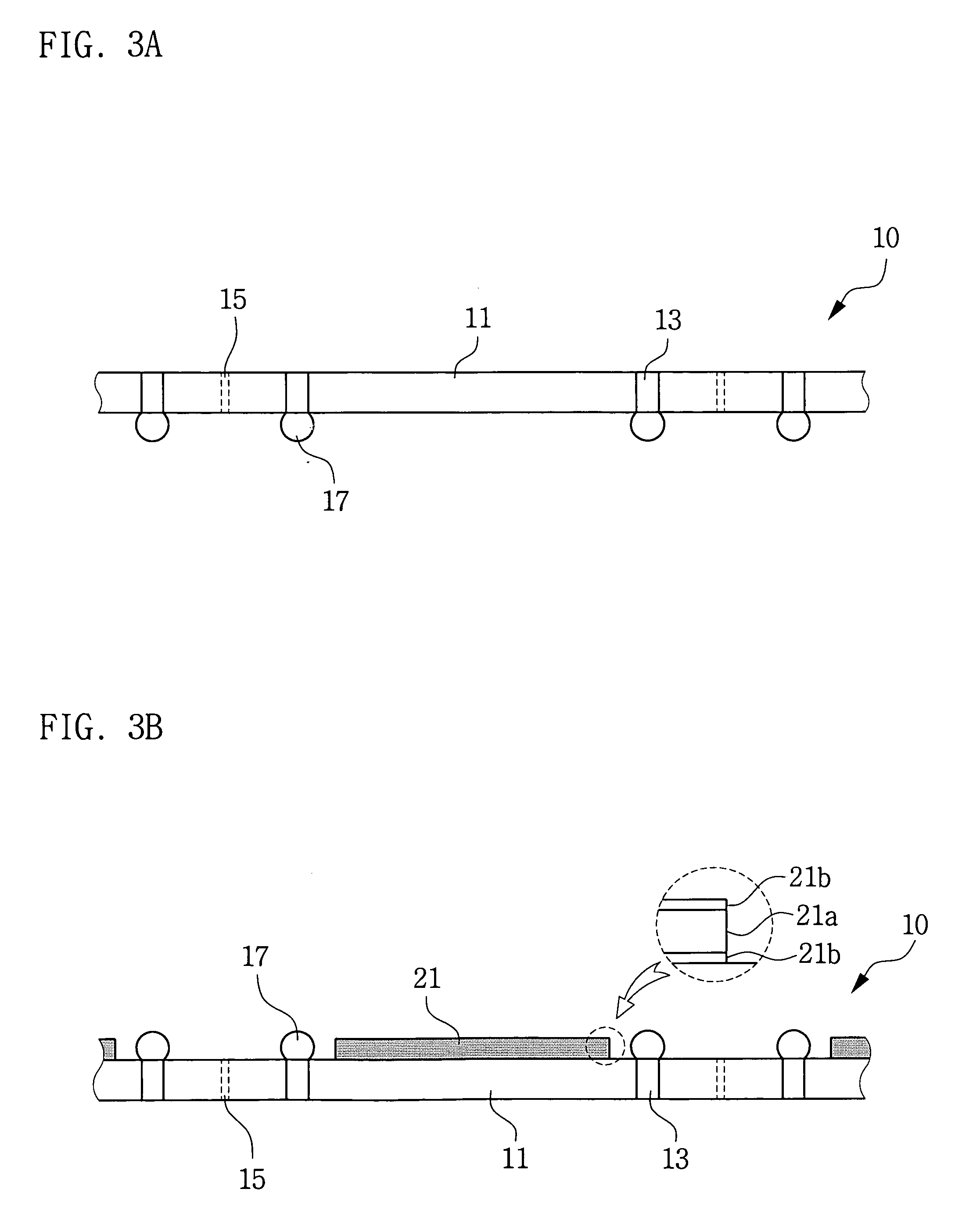
[0027]The present invention will now be described more fully hereinafter with reference to the accompanying drawings, in which exemplary embodiments of the invention are illustrated. In light of this detailed description, those of ordinary skill in the art will appreciate that this invention may be embodied in many different forms and should not, therefore, be construed as limited to the particular exemplary embodiments set forth herein. Rather, these exemplary embodiments are provided so that this disclosure will be thorough and complete, and will fully convey the scope of the invention to those skilled in the art.

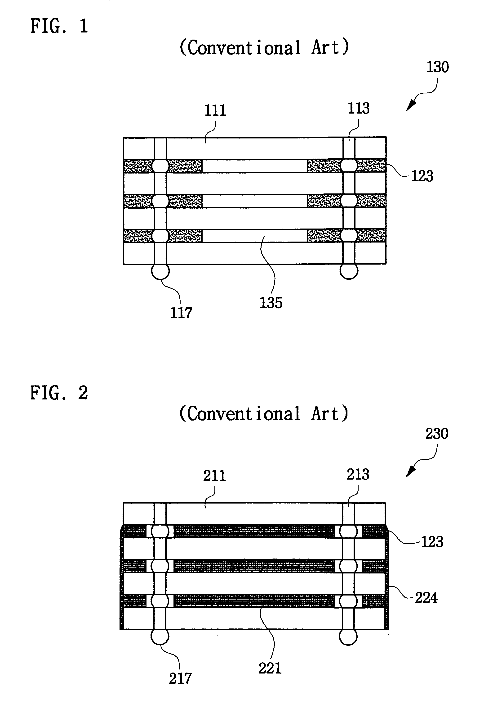
[0028]In the description, well-known structures and conventional processes have not been described or illustrated in detail to avoid obscuring the present invention. It will be appreciated that for simplicity and clarity of illustration, some elements illustrated in the figures have not necessarily been drawn to scale. For example, the dimensions of some of the elements h...


PUM


Abstract

Provided is a method for manufacturing WLCSP devices that includes preparing at least two wafers, each wafer having a plurality of corresponding semiconductor chips, each semiconductor chip having through electrodes formed in the peripheral surface region, forming or applying a solid adhesive region to a central surface region, stacking a plurality of wafers and attaching corresponding chips provided on adjacent wafers with the solid adhesive region and connecting corresponding through electrodes of adjacent semiconductor chips, dividing the stacked wafers into individual chip stack packages, and injecting a liquid adhesive into a space remaining between adjacent semiconductor chips incorporated in the resulting chip stack package. By reducing the likelihood of void regions between adjacent semiconductor chips, it is expected that a method according to the exemplary embodiments of the present invention exhibit improved mechanical stability and reliability.

Description

CROSS REFERENCE TO RELATED APPLICATIONS[0001]This U.S. non-provisional application claims priority under 35 U.S.C. § 119 of Korean Patent Application No. 2004-45567, filed on Jun. 18, 2004, the entire contents of which are incorporated herein by reference.BACKGROUND OF THE INVENTION[0002]1. Field of the Invention[0003]The present invention relates to a method for manufacturing a wafer level chip stack package.[0004]2. Description of the Related Art[0005]The electronic industry is continually seeking methods, techniques and designs that will result in the manufacture of electronic products that are smaller, lighter, faster, more efficient, operate at higher speeds, provide multiple functions and / or result in improved performance, at an effective cost. One of the methods that has been used for attaining such goals is improved package assembly techniques that have resulted in the development of new types of packages such as chip scale or chip size packages (CSP). The CSPs may be manufa...

Claims


Application Information

Patent Timeline
Patent Type & Authority Patents(United States)
IPC IPC(8): H01L21/44H01L21/48H01L21/56H01L21/60H01L21/98H01L23/31H01L23/48H01L25/065
CPCH01L21/563H01L23/481H01L24/32H01L25/0657H01L25/50H01L24/29H01L23/3114H01L23/3128H01L24/81H01L2224/16145H01L2224/274H01L2224/73203H01L2224/8121H01L2224/81815H01L2224/83191H01L2224/83194H01L2225/06513H01L2225/06541H01L2225/06582H01L2924/01029H01L2924/01079H01L2924/14H01L2924/15311H01L2924/15331H01L2224/32225H01L2224/32145H01L2924/01006H01L2924/01033H01L2924/3511H01L2224/16225H01L2224/73204H01L2924/00H01L2224/05573H01L2224/13025H01L2224/2612H01L2924/12042H01L23/48
Inventor KIM, SOON-BUMKIM, UNG-KWANGLEE, KANG-WOOKJEONG, SE-YOUNGSONG, YOUNG-HEESIM, SUNG-MIN
Owner SAMSUNG ELECTRONICS CO LTD
Why Eureka
Try Eureka