Semiconductor device and method for manufacturing the same

a semiconductor device and semiconductor technology, applied in the direction of semiconductor devices, basic electric elements, electrical appliances, etc., can solve the problems of increasing the junction capacitance of the source/drain region, the leakage current of the junction, etc., to reduce the junction leakage current and junction capacitance, improve the characteristics of the semiconductor device, and shorten the channel

Inactive Publication Date: 2006-12-19
SK HYNIX INC
View PDF10 Cites 14 Cited by
  • Summary
  • Abstract
  • Description
  • Claims
  • Application Information

AI Technical Summary

Benefits of technology

[0015]It is an object of the present invention to provide a semiconductor device and method for manufacturing the same wherein one side of a source and drain region and a portion of a channel region are disposed on a buried oxide layer formed on a semiconductor substrate and the side of the source and drain region and another portion of the channel region are disposed on a Si epitaxial layer formed on a semiconductor substrate to reduce junction leakage current and junction capacitance and suppress a short channel effect thereby improving characteristics of the semiconductor device.

Problems solved by technology

Moreover, the source / drain region is electrically connected to the semiconductor substrate resulting in increase in junction leakage current and junction capacitance of the source / drain region.

Method used


Image

  • Semiconductor device and method for manufacturing the same
  • Semiconductor device and method for manufacturing the same
  • Semiconductor device and method for manufacturing the same

Examples


Embodiment Construction

[0050]Reference will now be made in detail to exemplary embodiments of the present invention. Wherever possible, the same reference numbers will be used throughout the drawings to refer to the same or like parts.

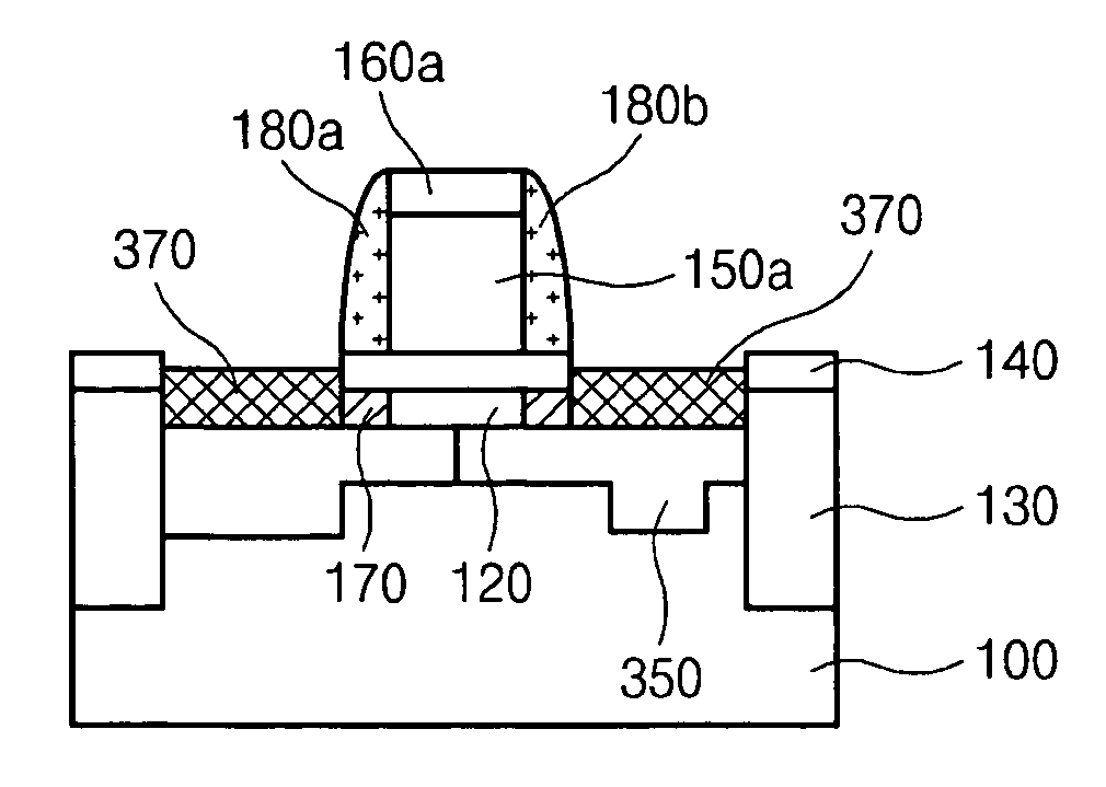
[0051]FIG. 4 is a layout illustrating a semiconductor device in accordance with the present invention, and FIGS. 5A through 5C are cross-sectional views illustrating a semiconductor device in accordance with a first preferred embodiment of the present invention respectively taken along the line X1–X1′, X2–X2′, and Y–Y′ of FIG. 4.

[0052]Referring to FIGS. 4 and 5A through 5C, the semiconductor device in accordance with the first preferred embodiment of the present invention comprises a semiconductor substrate 100 having an active region defined by a device isolation film 130, a gate structure having a first side 500a and a second side 500b. The gate structure comprises a stacked structure of a gate insulating film 140, a gate electrode 150a and a first CVD insulating film 160a...


PUM


Abstract

The present invention discloses improved semiconductor device and method for manufacturing wherein one side of a source and drain region and a portion of a channel region are disposed on a buried oxide layer formed on a semiconductor substrate and the side of the source and drain region and another portion of the channel region are disposed on a Si epitaxial layer formed on a semiconductor substrate.

Description

BACKGROUND OF THE INVENTION[0001]1. Field of the Invention[0002]The present invention relates to semiconductor device and method for manufacturing the same, and in particular to an improved semiconductor device and method for manufacturing the same wherein one side of a source and drain region and a portion of a channel region are disposed on a buried oxide layer formed on a semiconductor substrate and the side of the source and drain region and another portion of the channel region are disposed on a Si epitaxial layer formed on a semiconductor substrate to reduce a junction leakage current and junction capacitance and suppress a short channel effect thereby improving characteristics of the semiconductor device.[0003]2. Description of the Related Art[0004]FIGS. 1 and 2 are a layout illustrating a conventional semiconductor device, and a cross-sectional view of the conventional semiconductor device taken along the line I–I′ and II–II′ of FIG. 1, respectively.[0005]Referring to FIGS. ...

Claims


Application Information

Patent Timeline
Patent Type & Authority Patents(United States)
IPC IPC(8): H01L21/336
CPCH01L29/66772H01L29/78609H01L29/78621H01L21/02068H01L21/76876H01L29/41725H01L29/66719H01L29/7848
Inventor LEE, SANG DONKIM, YIL WOOKAHN, JIN HONG
Owner SK HYNIX INC
Why Eureka
Try Eureka