Optoelectronic package with wire-protection lid

a technology of optoelectronic packages and lids, which is applied in the direction of electrical apparatus casings/cabinets/drawers, semiconductor/solid-state device details, coupling device connections, etc., can solve the problems of easy short circuit to bonding wires, increased risk of light refraction, scattering, and wire collapse, and achieves the effect of improving the quality of the optoelectronic packag

Active Publication Date: 2006-12-26
ADVANCED SEMICON ENG INC
View PDF6 Cites 24 Cited by
  • Summary
  • Abstract
  • Description
  • Claims
  • Application Information

AI Technical Summary

Benefits of technology

[0008]An object of the present invention is to provide an optoelectronic package with a wire-protection lid, which mainly includes a substrate, a silicon die disposed on the substrate, a glass disposed on the silicon die, a plurality of bonding wires used for electrically connecting the substrate and the silicon die, and a silicon base lid with an opening. The silicon base lid is connected to the glass by anodic bonding to mask and protect the bonding wires. In addition, the opening of the silicon base lid is aligned with a light working area of the silicon die, to ensure a desirable light path. As for the optoelectronic package with wire-protection lid of the present invention, problems such as wire collapse and short circuit of the bonding wires due to forming the molding compound with molding can be avoided, thus the quality of the optoelectronic package is improved.
[0009]Another object of the present invention is to provide an optoelectronic package with a wire-protection lid. A silicon base lid has an opening and a recess, wherein the opening is communicated with a bottom surface of the recess, and the silicon base lid is connected to a glass on a silicon die by anodic bonding, such that the recess of the silicon base lid masks a plurality of bonding wires used for electrically connecting a substrate and the silicon die. The optoelectronic package with wire-protection lid of the present invention needs no rings to be disposed on the substrate, thus the components of the optoelectronic package are reduced.
[0010]Yet another object of the present invention is to provide an optoelectronic package with a wire-protection lid. An active surface of a silicon die includes a light working area, and a glass disposed on the silicon die has a surface bonding area surrounding the light working area, for connecting a silicon base lid by anodic bonding, such that an anodic bonding layer on the surface bonding area does not mask the light working area of the die, so as to avoid influencing the light path.

Problems solved by technology

However, the wire collapse and short circuit easily occur to the bonding wires 40 due to the molding pressure of the molding compound 50.
However, such a bonding wire protection method cannot ensure the transparent lid to be parallel to the active surface of the die and the glass carrier, therefore, when the light or image passes through the transparent lid and the glass carrier, the risks of light refraction, scattering, and defocusing will be increased, thereby the quality of the optoelectronic package is deteriorated.

Method used


Image

  • Optoelectronic package with wire-protection lid
  • Optoelectronic package with wire-protection lid
  • Optoelectronic package with wire-protection lid

Examples


first embodiment

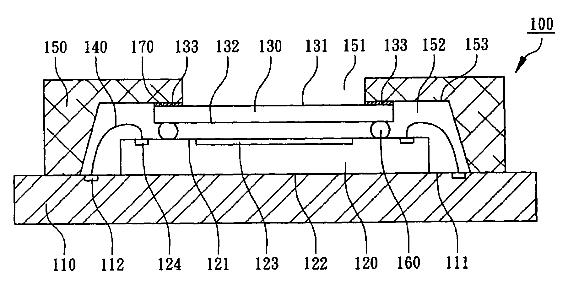
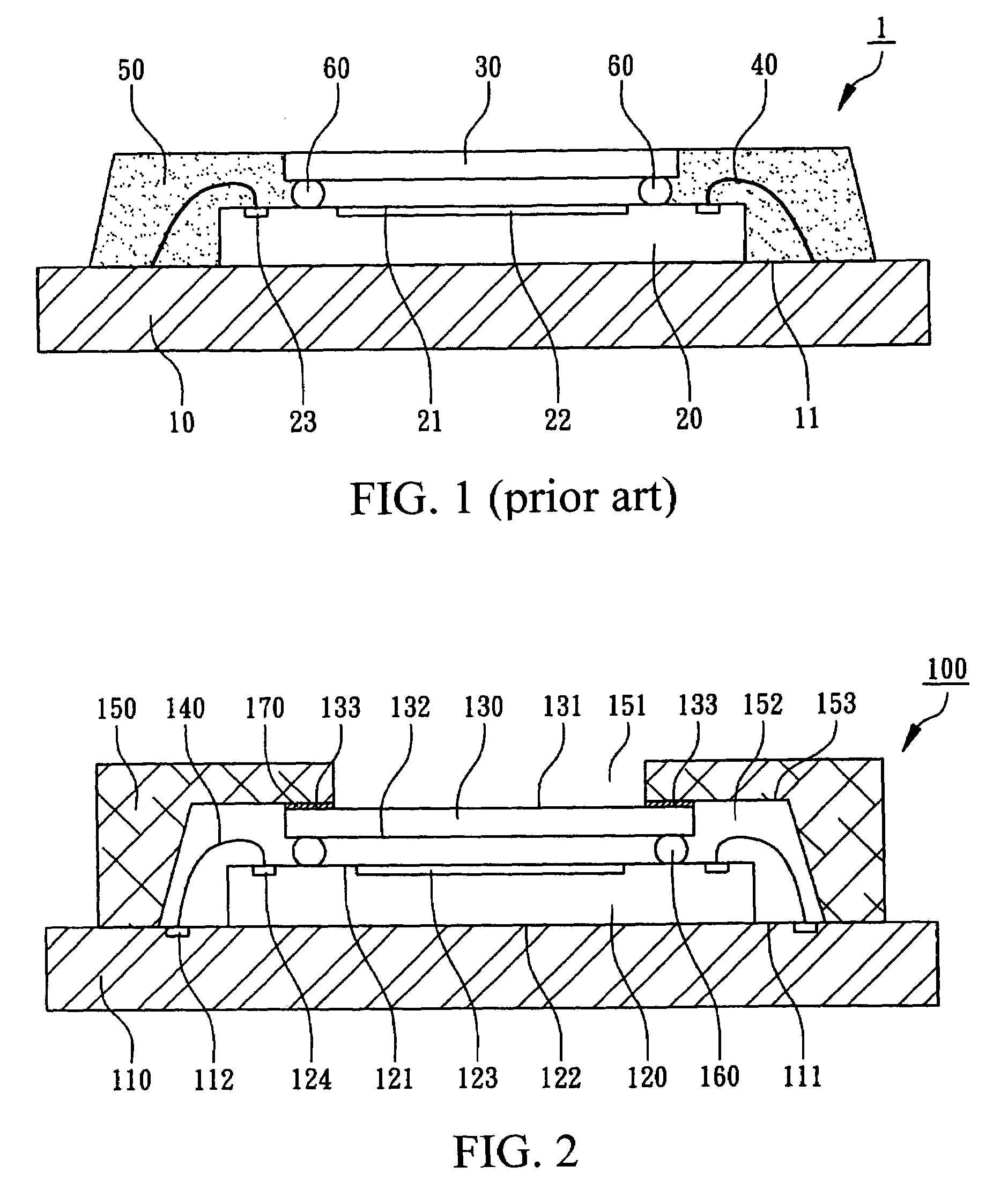
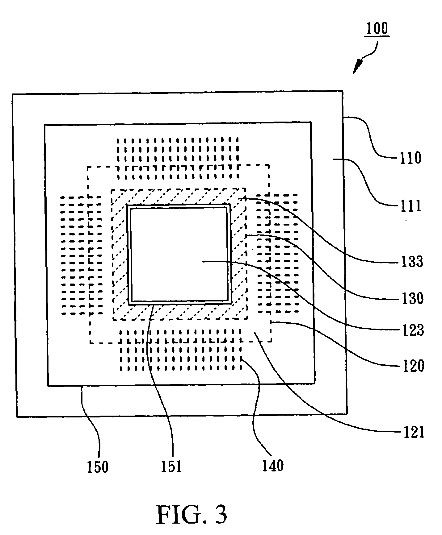
[0020]In the present invention, FIG. 2 is a schematic cross-sectional view of an optoelectronic package 100 with a wire-protection lid, and FIG. 3 is a top view of the optoelectronic package 100. Referring to FIG. 2, the optoelectronic package 100 mainly includes a substrate 110, a silicon die 120, a glass 130, a plurality of bonding wires 140, and a silicon base lid 150, wherein the substrate 110 has a top surface 111 with a plurality of connecting pads 112 being formed thereon. The substrate 110 can be a ceramic circuit board or another chip carrier.

[0021]The silicon die 120 has an active surface 121 and a back surface 122, wherein the active surface 121 includes a light working area 123 formed with a plurality of optical elements (not shown), and a plurality of pads 124 is formed on the active surface 121, and is disposed on other areas outside the light working area 123, for example, the edge area of the active surface 121. In the present embodiment, the silicon die 120 is a mic...

second embodiment

[0028]In the present invention, referring to FIG. 6, an optoelectronic package 200 with a wire-protection lid can be applied to various forms of optoelectronic products, which mainly includes a substrate 210, a silicon die 220, a glass 230, a plurality of bonding wires 240, and a silicon base lid 250. The substrate 210 has a top surface 211 with a plurality of connecting pads 212 being formed thereon.

[0029]The silicon die 220 has an active surface 221 and a back surface 222. The active surface 221 of the silicon die 220 includes a light working area 223, and a plurality of pads 224 is formed on the active surface 221. In the present embodiment, the silicon die 220 is an image sensor chip, and the light working area 223 is formed with a plurality of image sensor elements (not shown).

[0030]In the present embodiment, the glass 230 is adhered and connected to the active surface 221 of the silicon die 220 with a transparent adhesive 260. The silicon die 220 is disposed on the top surface...


PUM


Abstract

An optoelectronic package with a wire-protection lid is provided. An active surface of a silicon die includes a light working area. The silicon die is disposed on a substrate and electrically connected to the substrate through a plurality of bonding wires. A glass is disposed on the active surface of the silicon die. A silicon base lid with an opening is located above the substrate and connected to the glass by anodic bonding to mask the bonding wires. In addition, the opening of the silicon base lid is aligned with the light working area of the silicon die.

Description

CROSS-REFERENCE TO RELATED APPLICATIONS[0001]This non-provisional application claims priority under 35 U.S.C. § 119(a) on Patent Application No(s). 094105474 filed in Taiwan, R.O.C. on Feb. 23, 2005, the entire contents of which are hereby incorporated by reference.BACKGROUND OF THE INVENTION[0002]1. Field of Invention[0003]The present invention relates to an optoelectronic package, and more particularly, to an optoelectronic package with a wire-protection lid.[0004]2. Related Art[0005]Conventional optic components are manufactured on a semiconductor wafer in bulk, and an optoelectronic package process is carried out after the wafer is cut into dies. Since bonding wires are generally used to electrically connect the dies to the substrate in the conventional optoelectronic package process, appropriate protection of the bonding wires is required. Recently, a method for protecting the bonding wire of an optoelectronic package is to protect the bonding wires by sealing them with a moldi...

Claims


Application Information

Patent Timeline
Patent Type & Authority Patents(United States)
IPC IPC(8): H05K5/06H01L23/02
CPCB81B7/0067H01L31/0203H01L33/483H01L2224/48091H01L2224/48227H01L2924/01079H01L2924/00014H01L2224/45144H01L2924/00H01L2924/10253H01L2924/18161H01L2224/16145H01L2924/00011H01L2224/0401
Inventor HSU, CHAIN-HAU
Owner ADVANCED SEMICON ENG INC
Why Eureka
Try Eureka