Contact having multiple contact beams

a contact beam and contact technology, applied in the direction of coupling contact members, fixed connections, coupling device connections, etc., can solve the problems of limited signal transmission capacity, large contact volume, and large space occupied by contacts within the sock

Inactive Publication Date: 2007-01-02
TE CONNECTIVITY CORP
View PDF8 Cites 33 Cited by
  • Summary
  • Abstract
  • Description
  • Claims
  • Application Information

AI Technical Summary

Benefits of technology

[0006]Moreover, as contacts are made smaller, electrical signals encounter more resistance when traveling through the contacts and thus the socket. High resistance causes the contacts to generate heat as electrical signals pass therethrough which can damage surrounding parts and shorten product life. Additionally, more energy is required to convey electrical signals through high resistance contacts which causes the electronic device to consume more energy.

Problems solved by technology

The contacts are large and take up a large amount of space within the socket.
The socket thus carries a limited number of contacts and has a limited capacity to transmit signals between the processor and the circuit board.
If the shorter, smaller contact beams are overly deflected, they become permanently deformed.
Larger, longer contact beams may require too much force to be properly joined to the processor.
As the contact beams are positioned closer and closer, the EM fields begin to interfere with the performance of adjacent contact beams.
This interference appears as an increase in the inductance of the contacts.
Moreover, as contacts are made smaller, electrical signals encounter more resistance when traveling through the contacts and thus the socket.
High resistance causes the contacts to generate heat as electrical signals pass therethrough which can damage surrounding parts and shorten product life.
Additionally, more energy is required to convey electrical signals through high resistance contacts which causes the electronic device to consume more energy.

Method used


Image

  • Contact having multiple contact beams
  • Contact having multiple contact beams
  • Contact having multiple contact beams

Examples


Embodiment Construction

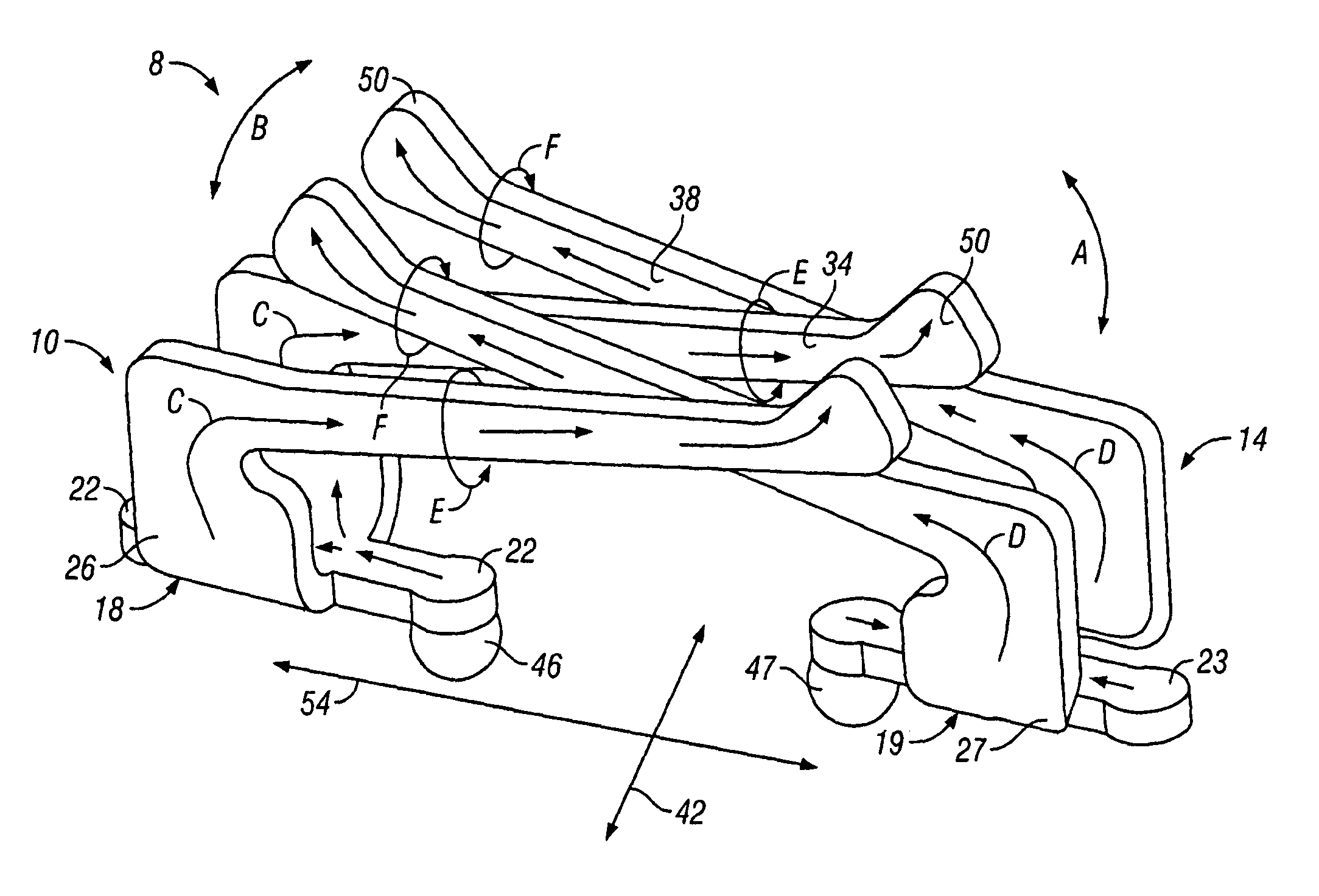
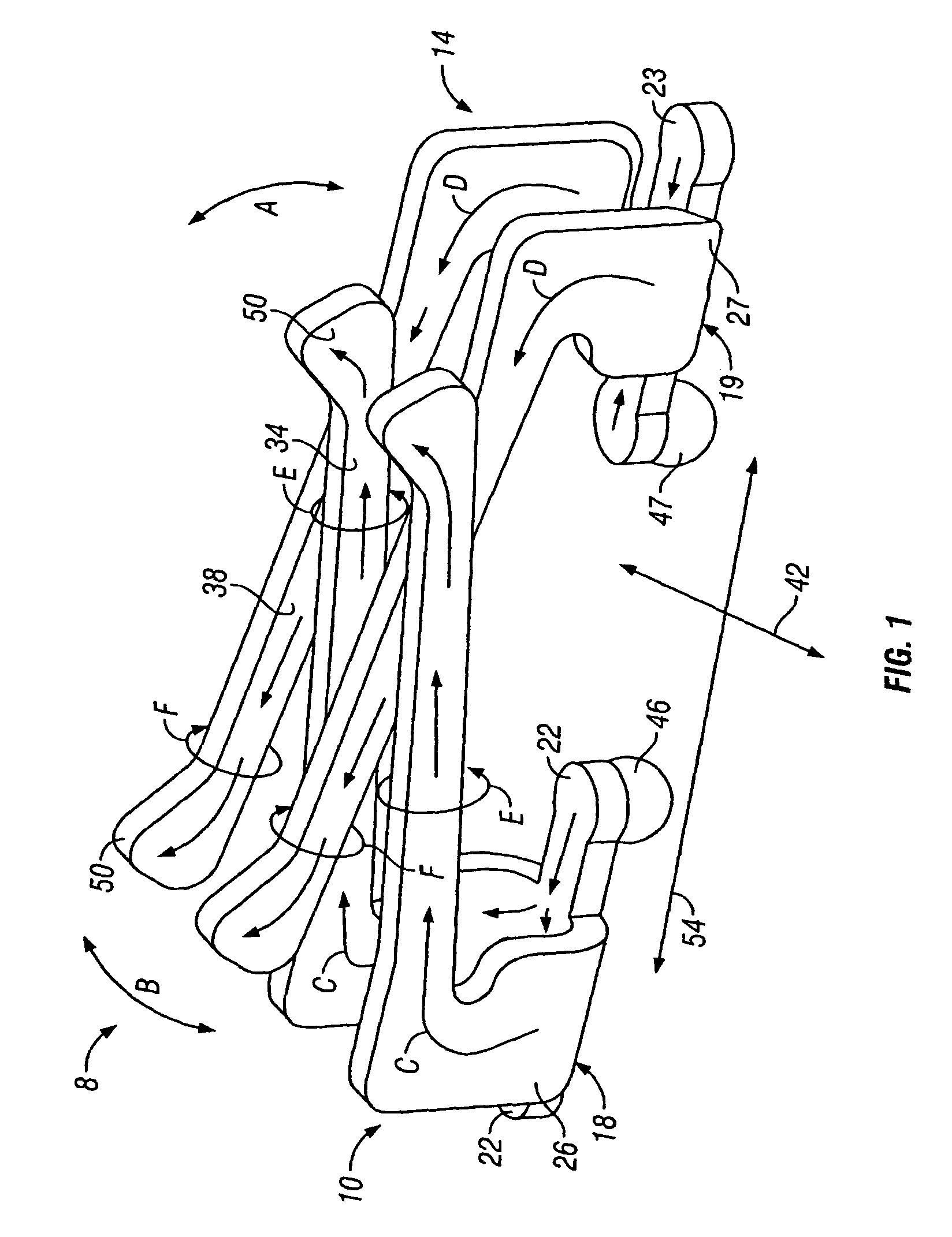
[0018]FIG. 1 illustrates an isometric view of a contact 8 having contact elements 10 and 14 arranged in an interleaved, overlapping manner according to an embodiment of the present invention. The contact elements 10 and 14 having base portions 18 and 19 with solder ball paddles 22 and 23 on opposite sides thereof. The solder ball paddles 22 and 23 carry solder balls 46 and 47. The solder ball paddles 22 and 23 comprise flexible termination leads having pads on the outer ends thereof. Optionally, the base portions 18 and 19 may have more or fewer than two solder ball paddles 22 and 23. As shown in FIG. 1, the base portions 18 and 19 are arranged parallel to a longitudinal axis 54. The contact elements 10 and 14 each have support plates 26 and 27 formed on opposite sides of the base portions 18 and 19. Contact beams 34 and 38 are formed with the support plates 26 and 27, respectively, and are thin, flexible and oriented in parallel planes. The contact beams 34 and 38 are formed to nor...


PUM


Abstract

An electrical socket is provided that holds an array of contacts. Each contact includes first and second contact elements that are configured to be joined in an electrically common manner. The first and second contact elements have first and second contact beams, respectively, that are oriented to project toward one another and to overlap. The first and second contact elements each have base portions that are formed separate from one another and are configured to be joined to a common conductive path on the circuit board.

Description

BACKGROUND OF THE INVENTION[0001]The present invention generally relates to a surface mount contact configured to be carried in an electrical component, such as a socket. More particularly, the present invention relates to a surface mount contact which has multiple contact beams.[0002]Contacts are used in a variety of applications to connect conductive members, such as processors, circuit boards and the like. In many applications, the contacts are held in a housing such as a socket. For example, a socket is generally used to connect a processor to a circuit board. The typical socket includes a body having cavities that carry several flexible contacts. A land grid array (LGA) socket holds the contacts that have a flexible body formed at one end with a contact beam and attached at an opposite end to a solder ball. The contact beam extends upward from the cavity above the top surface of the body of the socket, while the solder ball extends downward from the cavity below the bottom surf...

Claims


Application Information

Patent Timeline
Patent Type & Authority Patents(United States)
IPC IPC(8): H01R4/48H01R12/00H01R12/57H01R13/24
CPCH01R13/2492H01R12/57
Inventor BROWN, JOHN BOSSERTMCALONIS, MATTHEW RICHARDMCCLELLAN, JUSTIN SHANEMARTIN, DAVID CHARLESTAYLOR, ATTALEE S.CONNER, TROY EVERETTE
Owner TE CONNECTIVITY CORP
Why Eureka
Try Eureka