Group III nitride compound semiconductor light-emitting element

a technology of compound semiconductors and light-emitting elements, which is applied in the direction of semiconductor/solid-state device manufacturing, semiconductor devices, electrical devices, etc., can solve the problems of difficult to produce led lamps, difficult to control the thickness of the respective layers in the multi-layer crystalline film strictly, etc., and achieve good yield and reduce the characteristic of light-emitting elements. , the effect of large variation

Inactive Publication Date: 2007-01-02
TOYODA GOSEI CO LTD
View PDF15 Cites 44 Cited by
  • Summary
  • Abstract
  • Description
  • Claims
  • Application Information

AI Technical Summary

Benefits of technology

[0010]According to such a configuration, light is scattered when radiated out because light emitted from the light-emitting layer-containing layer is radiated out through the light-scattering surface. That is, light which has passed through the light-emitting element and reached a light-emitting surface is scattered on the light-emitting surface so as to be radiated out (at random radiation angles). The form of radiation of the light is made uniform by the scattering on the light-emitting surface, so that variation in the characteristic of the light-emitting element is reduced greatly. Hence, when the light-emitting element according to the invention is used for forming an LED lamp, the LED lamp having desired characteristic can be produced with a good yield.

Problems solved by technology

It is, however, difficult to control the thicknesses of the respective layers in the multilayer crystalline film strictly.
Hence, there has been a problem that the characteristic varies from one light-emitting element to another light-emitting element.
Hence, it has been difficult to produce such an LED lamp having desired characteristic with a good yield.

Method used


Image

  • Group III nitride compound semiconductor light-emitting element
  • Group III nitride compound semiconductor light-emitting element
  • Group III nitride compound semiconductor light-emitting element

Examples


Embodiment Construction

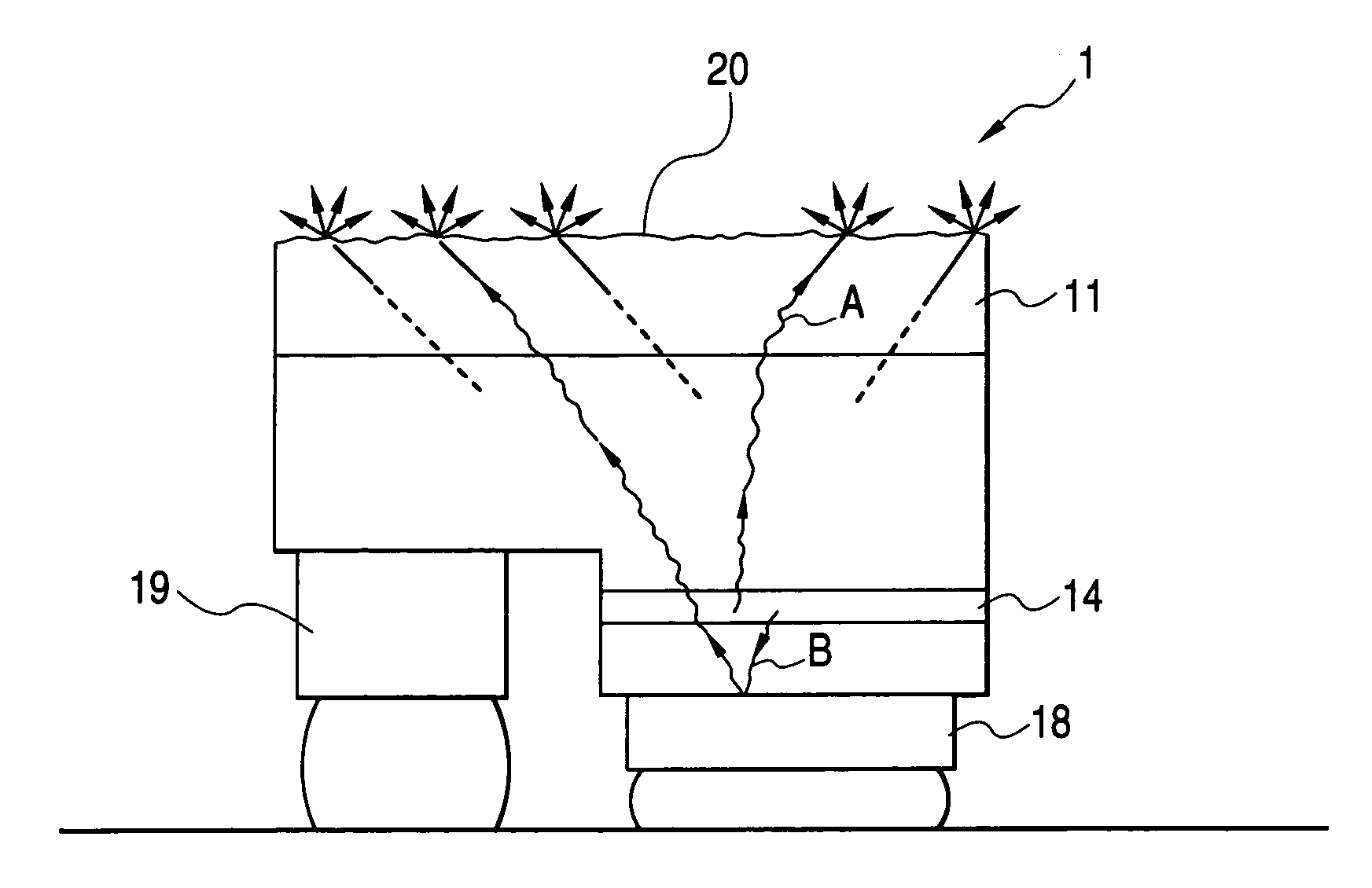
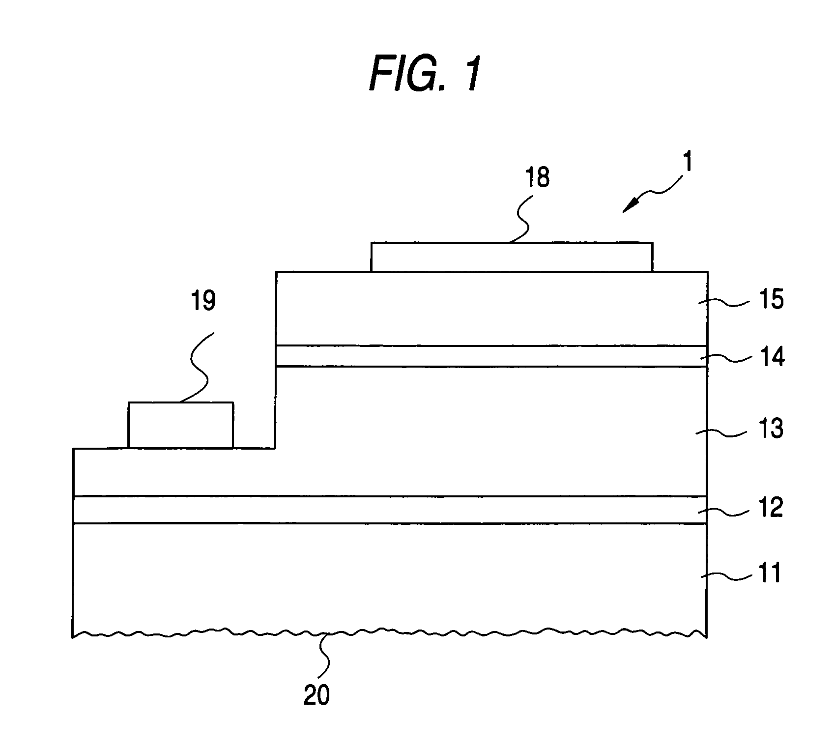
[0019]The Group III nitride compound semiconductor light-emitting element according to the invention is a flip chip type light-emitting element including a substrate, and Group III nitride compound semiconductor layers including a light-emitting layer and laminated on the substrate. The “flip chip type light-emitting element” means a light-emitting element used in a flip chip type light-emitting device, that is, it means a light-emitting element used after mounted on a support (such as a substrate) through its mount surface on which p-side and n-side electrodes are formed. In other words, a flip chip type light-emitting device can be formed by use of the light-emitting element according to the invention. In the light-emitting element according to the invention, emitted light is radiated from a substrate side, that is, from a surface opposite to the surface in which electrodes are formed.

[0020]The constituent members of the Group III nitride compound semiconductor light-emitting elem...


PUM

PropertyMeasurementUnit
particle sizeaaaaaaaaaa
thicknessaaaaaaaaaa
surface roughness Raaaaaaaaaaa

Abstract

In a flip chip type Group III nitride compound semiconductor light-emitting element, a surface of a substrate serving as a light-emitting surface is formed as a rough surface so that radiated light is scattered by the surface.

Description

[0001]The present application is based on Japanese Patent Application No. 2001-170909, which is incorporated herein by reference.BACKGROUND OF THE INVENTION[0002]1. Field of the Invention[0003]The present invention relates to a Group III nitride compound semiconductor light-emitting element and particularly to a flip chip type Group III nitride compound semiconductor light-emitting element.[0004]2. Description of the Related Art[0005]FIG. 6 shows a flip chip type light-emitting element 100 having a related-art configuration. The light-emitting element 100 includes a support 101, and a plurality of Group III nitride compound semiconductor layers 102 laminated on the substrate 101. The light-emitting element 100 has a surface in which electrodes 103 and 104 are formed and which serves as a mount surface. The light-emitting element 100 is mounted on a support 105 through the mount surface when light-emitting element 100 is used. In the light-emitting element 100 configured as described...

Claims


Application Information

Patent Timeline
Patent Type & Authority Patents(United States)
IPC IPC(8): H01L33/00H01L33/10H01L33/12H01L33/32H01L33/62
CPCH01L33/22H01L33/32H01L2224/48091H01L2224/48247H01L2924/00014
Inventor UEMURA, TOSHIYAHASHIMURA, MASAKI
Owner TOYODA GOSEI CO LTD
Why Eureka
Try Eureka